Array substrate, manufacturing method thereof, and display device

An array substrate and substrate technology, applied in optics, instruments, electrical components, etc., can solve the problems of lower transmittance, loss of panel transmittance, increase of backlight cost, etc., to reduce the influence of transmittance and reduce light leakage The effect of the probability of occurrence

Active Publication Date: 2016-12-28
BOE TECH GRP CO LTD
View PDF8 Cites 3 Cited by
  • Summary
  • Abstract
  • Description
  • Claims
  • Application Information

AI Technical Summary

Problems solved by technology

However, when the array substrate and the color filter substrate are aligned to form a box, due to the limitation of alignment accuracy, alignment deviation is very easy to occur, and alignment deviation will cause light leakage, lower transmittance and other defects; if the black matrix is ​​made Wide enough to avoid these problems, but will lose the transmittance of the panel and increase the cost of the backlight

Method used


Image

  • Array substrate, manufacturing method thereof, and display device
  • Array substrate, manufacturing method thereof, and display device
  • Array substrate, manufacturing method thereof, and display device

Examples


Embodiment 1

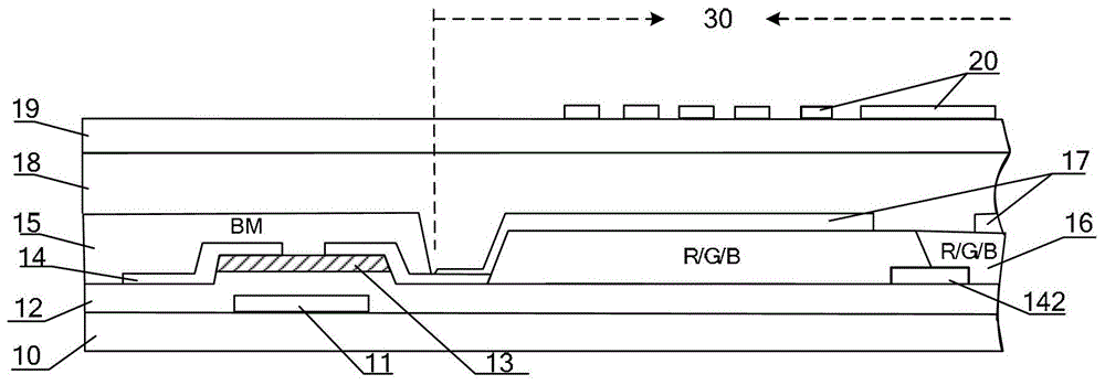
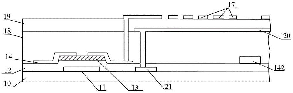
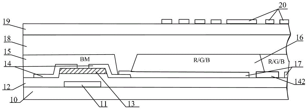
[0057] An embodiment of the present invention provides an array substrate, which includes: a substrate, a plurality of pixels formed on the substrate, and a black matrix separating the pixels;

[0058] Corresponding to the area where the black matrix is ​​located, the substrate is provided with a gate, a gate insulating layer, a semiconductor layer, a source electrode and a drain electrode;

[0059] The corresponding area of ​​the pixel is provided with a first electrode and a second electrode for generating an electric field to drive the liquid crystal, the second electrode is arranged above the first electrode, and further includes:

[0060] patterned color resist layer,

[0061] The color resistance layer is disposed between the gate insulating layer and the layer where the second electrode is located, and is distributed in a corresponding area of ​​the pixel.

[0062] In this embodiment, the gate, the gate insulating layer, the semiconductor layer, the source electrode an...

Embodiment 2

[0087] An embodiment of the present invention also provides a display device, which includes any one of the array substrates described in Embodiment 1. The display device may be any product or component with a display function such as a liquid crystal panel, an electronic paper, an OLED panel, a mobile phone, a tablet computer, a television, a monitor, a notebook computer, a digital photo frame, a navigator, and the like.

[0088] The display device described in this embodiment uses a color resist layer and a black matrix on the array substrate, so the influence of the alignment deviation between the array substrate and the color filter substrate on the transmittance can be reduced, so that the blocking area of ​​the black matrix can be reduced. Small, the transmittance and brightness of the display device can be improved.

Embodiment 3

[0090] Such as Figure 4 with Figure 5 As shown, the embodiment of the present invention also provides a method for manufacturing an array substrate, including:

[0091] 101. Form a gate metal layer on the substrate 10, and use a patterning process to form patterns of gate lines and gates;

[0092] Optionally, in this step, a magnetron sputtering or thermal evaporation film forming method is firstly used to deposit a gate metal layer on the substrate 10 , wherein. The material for preparing the gate metal layer may be selected from one or more of molybdenum, aluminum, chromium and copper.

[0093] Optionally, the patterning process described in this embodiment refers to the entire photolithography process of forming patterns on the substrate through steps such as gluing, exposure under the mask plate, and etching, which is also called a masking process.

[0094] 102. Form patterns of the gate insulating layer 12, the semiconductor layer 13, and the source-drain electrode l...


PUM


Abstract

The invention discloses an array substrate, a manufacturing method thereof, and a display device, relating to the field of display, which can reduce the influence of the alignment deviation between the array substrate and the color filter substrate on the transmittance, and avoid light leakage caused by the alignment deviation. The array substrate of the present invention includes: a substrate, a plurality of pixels formed on the substrate and a black matrix separating the pixels; corresponding to the area where the black matrix is ​​located, the substrate is provided with a gate, a gate insulating layer, a semiconductor layer, a source electrode and a drain electrode. Pole; the corresponding area of ​​the pixel is provided with a first electrode and a second electrode for generating an electric field to drive the liquid crystal, the second electrode is arranged above the first electrode, and also includes: a patterned color resistance layer, the color resistance layer is set Between the gate insulating layer and the layer where the second electrode is located, and distributed in the corresponding area of ​​the pixel. The invention is used to improve the display device and can increase the transmittance of the display device.

Description

technical field [0001] The present invention relates to the display field, in particular to an array substrate, a manufacturing method thereof, and a display device. Background technique [0002] Due to its advantages of light weight, low power consumption, low radiation, and a large amount of space saving, liquid crystal displays have replaced traditional cathode ray tube displays and are widely used in various display fields, such as households, public places, offices, and personal electronics. products etc. [0003] The current manufacturing process of liquid crystal panels is to separately manufacture the array (Array) substrate and the color filter (Color Filter) substrate, and then align the array substrate and the color filter substrate to form a cell (Cell). However, when the array substrate and the color filter substrate are aligned to form a box, due to the limitation of alignment accuracy, alignment deviation is very easy to occur, and alignment deviation will ca...

Claims


Application Information

Patent Timeline
Patent Type & Authority Patents(China)
IPC IPC(8): G02F1/1335
CPCG02F1/133514G02F1/134309G02F1/136209G02F1/134372G02F1/136222H10K50/85H10K59/12G02F1/1343G02F1/1368H01L27/124H01L27/1259
Inventor 崔贤植李会徐智强严允晟
Owner BOE TECH GRP CO LTD
Why Eureka
Try Eureka