Supercharge Your Innovation With Domain-Expert AI Agents!

Novel high-density multilayer circuit chip flip encapsulation structure and manufacturing method

A multi-layer circuit, flip-chip packaging technology, used in circuits, semiconductor/solid-state device manufacturing, electrical components, etc. To ultra-thin package design and other issues, to achieve the effect of small thermal expansion coefficient, improved safety, and high strength

Active Publication Date: 2013-09-18
江阴芯智联电子科技有限公司
View PDF4 Cites 2 Cited by
  • Summary
  • Abstract
  • Description
  • Claims
  • Application Information

AI Technical Summary

Problems solved by technology

[0005] 2. Because there is an extra layer of glass fiber board core layer, the thickness is about 100~150μm, so it is impossible to achieve ultra-thin packaging design;
[0006] 3. Glass fiber itself is a kind of foaming material, so it is easy to absorb moisture and moisture due to the storage time and environment, which directly affects the safety capability or reliability level of reliability;
[0007] 4. The connection between the circuit layers is made by laser drilling, and then copper plating is carried out. The aperture formed by laser drilling is large, and it is difficult to achieve high-density design and manufacture.

Method used


Image

  • Novel high-density multilayer circuit chip flip encapsulation structure and manufacturing method
  • Novel high-density multilayer circuit chip flip encapsulation structure and manufacturing method
  • Novel high-density multilayer circuit chip flip encapsulation structure and manufacturing method

Examples


Embodiment Construction

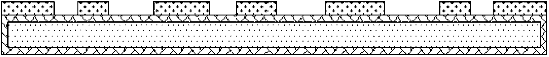
[0085] The present invention is a novel high-density multilayer circuit chip flip-chip packaging structure, which includes a circuit layer 10, a chip 2 and a circuit layer 11, and the circuit layer 10 and the circuit layer 11 are connected by copper The column layer 5 is connected, and the insulating material 6 is filled between the copper column layer 5 and the copper column layer 5 and between the circuit layer 10 and the circuit layer 10, and the circuit layer 10 and the insulating material 6 is provided with an outer ink layer 9 on the back. The outer ink layer 9 is exposed and developed to expose the outer pin 7 on the back of the circuit layer 10. The outer pin 7 is provided with a metal ball 8. The second layer of circuit Layer 11 is provided with inner pins 12 on the flip-chip soldering area 3 on the front side, and an inner ink layer 1 is arranged around the two-layer circuit layer 11 and inner pins 12, and the chip 2 is flip-chip on the front side of inner pins 12, so...


PUM


Abstract

The invention relates to a novel high-density multilayer circuit chip flip encapsulation structure and a manufacturing method thereof. The encapsulation structure comprises a first circuit layer (10), a chip (2) and a second circuit layer (11), wherein an external ink layer (9) is arranged on the back sides of the first circuit layer (10) and an insulation material layer (6), a metallic ball (8) is arranged at the position of an outer pin (7), an inner pin (12) is arranged on the front side of the second circuit layer (11), an internal ink layer (1) is arranged on the periphery of the second circuit layer (11) and the inner pin (12), the chip (2) is mounted on the front side of the inner pin (12) upside down, and molding compound (4) is enveloped on the periphery of the chip (2). The novel high-density multilayer circuit chip flip encapsulation structure and the manufacturing method thereof have the beneficial effects that the thickness of a chip encapsulation carrier plate is reduced, and the ultra-thin high-density encapsulation is realized; the level of reliability is improved; the technical capacity on high-density circuit is truly achieved; the warping problem of a traditional substrate during the encapsulation process is radically solved.

Description

technical field [0001] The invention relates to a novel high-density multilayer circuit chip flip-chip packaging structure and a manufacturing method, belonging to the technical field of semiconductor packaging. Background technique [0002] The current high-density substrate packaging structure such as Figure 25 As shown, the manufacturing process is mainly to form a multi-layer circuit board by stacking the core material of the glass fiber board by accumulating materials. The holes between the circuit layers are opened by laser drilling, and then the holes are plated to complete the electrical circuit board. connect. [0003] The above-mentioned current high-density substrate packaging structure has the following deficiencies and defects: [0004] 1. There is an extra layer of glass fiber material, and also the cost of an extra layer of glass fiber; [0005] 2. Because there is an extra layer of glass fiber board core layer, the thickness is about 100~150μm, so it is im...

Claims


Application Information

Patent Timeline
IPC IPC(8): H01L23/498H01L23/31H01L21/48H01L21/56
CPCH01L24/97H01L2224/16H01L2224/97H01L2924/15311H01L2924/181
Inventor 陈灵芝夏文斌廖小景邹建安仰洪波
Owner 江阴芯智联电子科技有限公司
Features
  • R&D
  • Intellectual Property
  • Life Sciences
  • Materials
  • Tech Scout
  • Unparalleled Data Quality
  • Higher Quality Content
  • 60% Fewer Hallucinations
Learn More