Fast recovery diode and method for manufacturing fast recovery diode

A recovery diode and manufacturing method technology, applied in semiconductor/solid-state device manufacturing, electrical components, circuits, etc., can solve problems such as high reverse recovery voltage, adverse effects of circuits, and excellent reverse recovery

Active Publication Date: 2013-09-18
SHENZHEN ESPIRIT TECH
View PDF5 Cites 5 Cited by
  • Summary
  • Abstract
  • Description
  • Claims
  • Application Information

AI Technical Summary

Problems solved by technology

However, these technologies are often difficult to achieve an ideal compromise in the parameters of the fast recovery diode
For example, the diode with P-i-N structure can shorten the reverse recovery time, but the reverse recov...

Method used


Image

  • Fast recovery diode and method for manufacturing fast recovery diode
  • Fast recovery diode and method for manufacturing fast recovery diode
  • Fast recovery diode and method for manufacturing fast recovery diode

Examples


Embodiment Construction

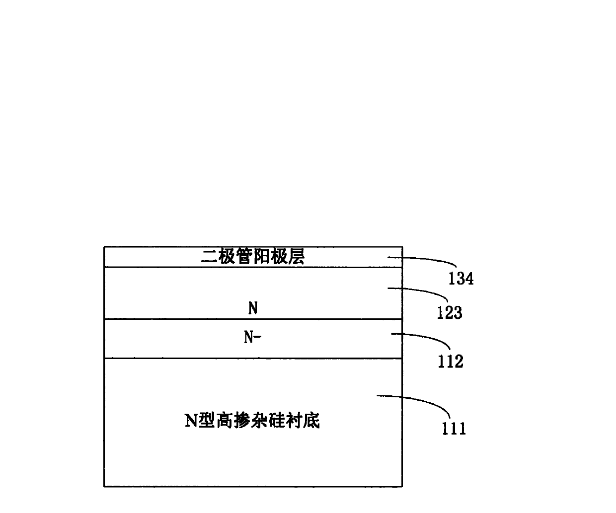
[0016] Please refer to figure 2 The preferred embodiment of the fast recovery diode of the present invention includes an N-type highly doped silicon substrate 111, a first N-type doped semiconductor layer 112, a second N-type doped semiconductor layer 123, and a diode anode layer 134 The first N-type doped semiconductor layer 112 is located between the second N-type doped semiconductor layer 123 and the N-type highly doped silicon substrate 111. The width of the first N-type doped semiconductor layer 112 is 5um to 50um, and the doping concentration is 5e12 / cm 3 -5e14 / cm 3 . The doping concentration of the second N-type doped semiconductor layer 123 is N D The width d of the second N-type doped semiconductor layer 123 satisfies formula (1):

[0017] Where ε in formula (1) r Is the dielectric constant of silicon, ε 0 Is the vacuum dielectric constant, e refers to the electric quantity of a single electron, V R It is the reverse bias voltage for normal operation, and EBV is the cr...


PUM

PropertyMeasurementUnit
Widthaaaaaaaaaa
Doping concentrationaaaaaaaaaa

Abstract

The invention provides a fast recovery diode, which comprises an N type high-doping silicon substrate, a first N type doping semiconductor layer, a second N type doping semiconductor layer and a diode anode layer, wherein the first N type doping semiconductor layer is positioned between the second N type doping semiconductor layer and the N type high-doping silicon substrate, and the doping concentration of the first N type doping semiconductor layer is lower than the doping concentration of the second N type doping semiconductor layer. The fast recovery diode can provide the sufficient current carrier concentration during the reverse recovery, so the current fall softness can be maintained. The invention also provides a method for manufacturing the fast recovery diode.

Description

Technical field [0001] The invention relates to a diode and a method for manufacturing the diode. Background technique [0002] With the development of power electronic technology, the application of various frequency conversion circuits and chopper circuits has been expanding. The main circuits in these power electronic circuits adopt either thyristors with commutation shutoff or new power electronics with self-shutdown capabilities. Devices require a diode with a short reverse recovery time connected in parallel to pass the reactive current in the load while suppressing the high voltage induced by the instantaneous reverse of the load current. [0003] Accordingly, a variety of fast recovery diodes with various characteristics have been pushed to the application market, such as sonic FRD (Fast Recovery Diodes) from IXYS, SPT+FRD from ABB, EMCON from Infineon, HEXFRED from IR and many more. [0004] Please refer to figure 1 , Which shows a fast recovery diode with a P-i-N structur...

Claims


Application Information

Patent Timeline
IPC IPC(8): H01L29/36H01L29/861H01L21/329
Inventor 贾会霞
Owner SHENZHEN ESPIRIT TECH
Why Eureka
Try Eureka