Polarization coupling device

A coupling device and polarization technology, applied in optical components, optics, instruments, etc., can solve the problems of incapable laser light source beam size compression, poor resistance to laser damage, inconvenient movement, etc., to improve beam quality and beam brightness, space pendulum The effect of simple placement and reduced space occupation

Inactive Publication Date: 2013-09-25
INST OF SEMICONDUCTORS - CHINESE ACAD OF SCI
View PDF7 Cites 16 Cited by
  • Summary
  • Abstract
  • Description
  • Claims
  • Application Information

AI Technical Summary

Problems solved by technology

[0006] However, for the above-mentioned polarization coupling device, it can only compress the beam size of two laser light sources, but cannot compress the beam size of one laser light source
In addition, there are strict requirements on the space placement of the laser light source, the structure of the whole system is not compact enough, it takes up a lot of space, and it is inconvenient to move
In addition, the polarization cube splitting interface of the polarization coupling device is generally connected by ordinary glue, and the ability to resist laser damage is poor

Method used


Image

  • Polarization coupling device
  • Polarization coupling device
  • Polarization coupling device

Examples


Embodiment Construction

[0024] In order to make the object, technical solution and advantages of the present invention clearer, the present invention will be described in further detail below in conjunction with specific embodiments and with reference to the accompanying drawings. It should be noted that, in the drawings or descriptions of the specification, similar or identical parts all use the same figure numbers. Implementations not shown or described in the accompanying drawings are forms known to those of ordinary skill in the art.

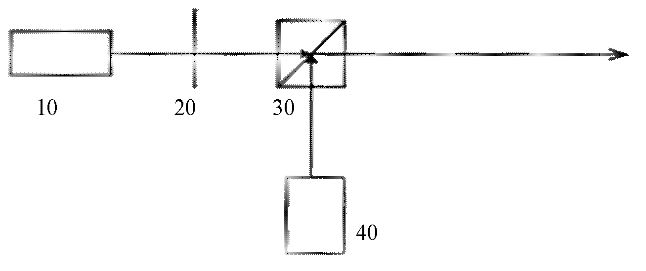
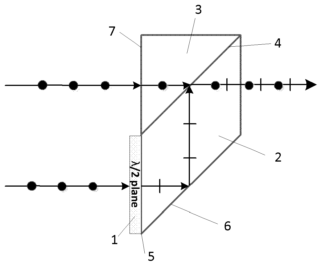
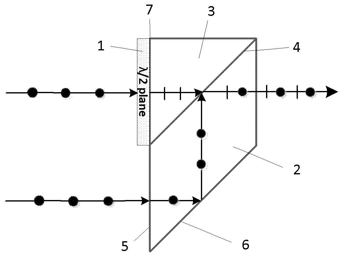
[0025] The invention provides a polarization coupling device. The polarization coupling device shrinks the output beam of the high-power semiconductor laser through right-angle prism, rhomboid prism, polarization beam splitting film layer and molecular bonding, thereby improving the brightness and beam quality of the output beam.

[0026] In an exemplary embodiment of the present invention, a polarization coupling device is provided. figure 2 It is a schematic s...


PUM


Abstract

The invention provides a polarization coupling device. The polarization coupling device comprises a rectangular prism, a rhombic prism and a 1 / 2 wave plate. A first right angle plane of the rectangular prism faces towards the direction of an incident laser. The length of a first long edge plane of the rhombic prism is equal to the length of an bevel edge plane of the rectangular prism, either the first long edge plane or the bevel edge plane or both the first long edge plane and the bevel edge plane are plated by a polarization spectroscopic film layer and are closely attached to the polarization spectroscopic film layer to form a polarizing beamsplitting interface. A second long edge plane of the rhombic prism is plated by a laser all reflective film, a first short edge plane of the rhombic prism faces the direction of the incident laser, and a second short edge plane of the rhombic prism serves as a laser sending plane. The 1 / 2 wave plate is located at the front end of a light path of the first right angle plane of the rectangular prism when the polarization spectroscopic film layer is an S polarized light high permeability P polarized light high reflective film, and the 1 / 2 wave plate is located at the front end of a light path of the first short edge plane of the rhombic prism when the polarization spectroscopic film layer is a P polarized light high permeability S polarized light high reflective film. According to the polarization coupling device, the size of a light beam of a single laser light source can be compressed.

Description

technical field [0001] The invention relates to the technical field of semiconductor lasers, in particular to a high damage threshold polarization coupling device for high-power semiconductor lasers. Background technique [0002] Semiconductor lasers have the advantages of high photoelectric conversion efficiency, small size, and long life. They are widely used in various fields, especially kilowatt-level high-power semiconductor lasers with high beam quality and high brightness. Medical and other fields have a wide range of applications and good development prospects. [0003] However, the output light of semiconductor lasers is incoherent in space. High-power semiconductor lasers have more light-emitting units, and the defects of poor beam quality and low brightness of the output light greatly limit its application and promotion. Therefore, improving beam quality and luminous brightness has become the key to the further development of high-power semiconductor lasers. [...

Claims


Application Information

Patent Timeline
Patent Type & Authority Applications(China)
IPC IPC(8): G02B27/28G02B27/09
Inventor 林学春王丽荣王宝华郭渭荣王祥鹏陈凯
Owner INST OF SEMICONDUCTORS - CHINESE ACAD OF SCI
Why Eureka
Try Eureka