
Patsnap Eureka
For R&D, Patsnap Eureka makes reading and utilizing patents & technical documents easy.
Patsnap Eureka AIR
Designed for self-driven R&D workflows. Generate viable solutions, solve complex R&D challenges, empower your innovation with AI.

Patsnap Eureka Materials
Designed for material experts only. Revolutionize your material R&D, from search, analyze, to developing new materials.

TechResearch
Generate reliable direction feasibility study reports for your R&D in just a few steps.

TechSeek
Discover and master advanced knowledge NOW. Basics, ideas, possibilities, all at once.

TechMind
As an expert in R&D Theories, TechMind can generates customized viable solutions instantly.

TechRisk
Analyze your overall solution with one click, know your potential R&D risks in advance.

TechMonitor
Get weekly tech updates, stay abreast of the latest tech innovations and key insights.
Light emitting diode (LED) with composite transparent conducting layer and preparation method thereof
A technology of light emitting diodes and transparent conductive layers, applied in circuits, electrical components, semiconductor devices, etc., can solve problems such as inability to effectively eliminate total reflection, and achieve the effects of low production cost, high controllability, and improved light extraction efficiency
- Summary
- Abstract
- Description
- Claims
- Application Information
AI Technical Summary
Problems solved by technology
Method used
Image

Examples
no. 1 example
[0054] The light emitting diode according to the first embodiment of the present invention and its manufacturing method will be described in detail below with reference to the accompanying drawings.
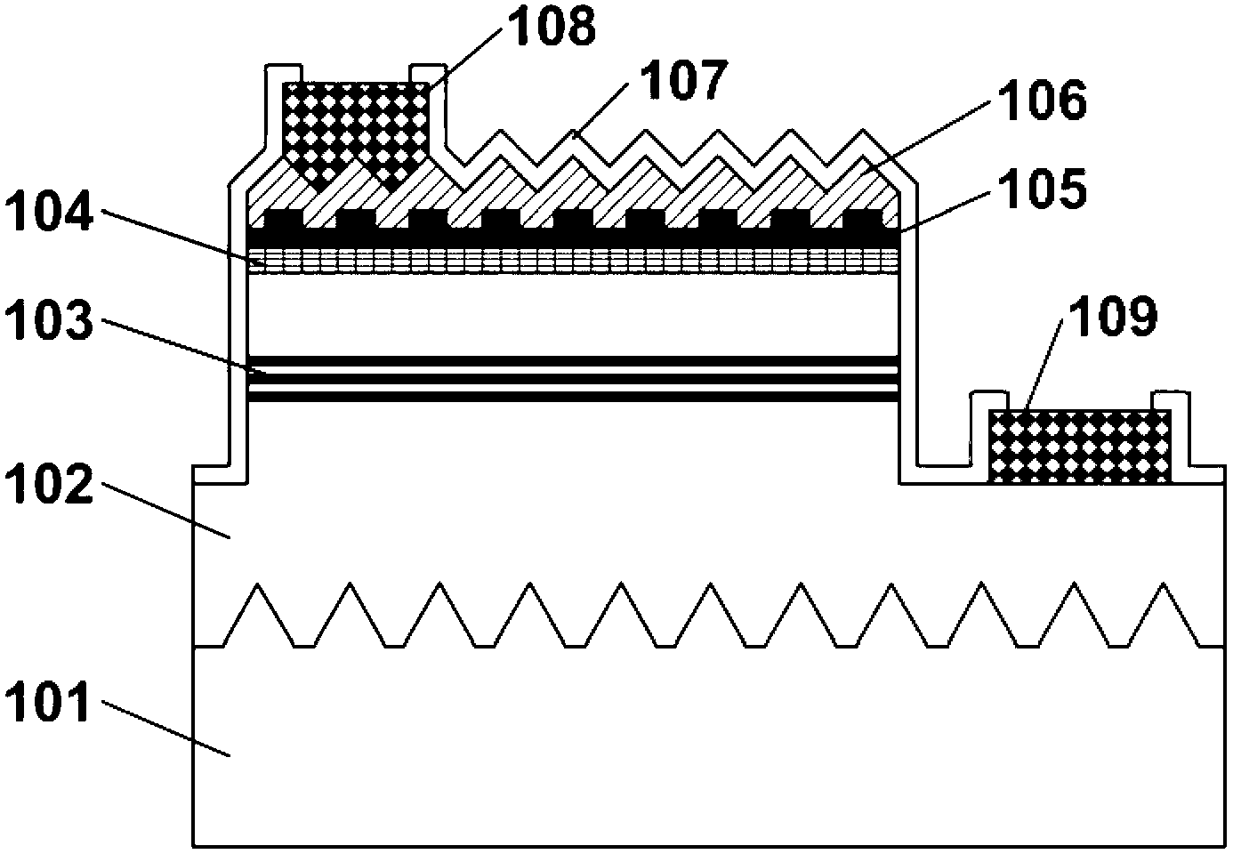
[0055] The light emitting diode according to the first embodiment includes a Group-III nitride epitaxial layer, a composite transparent conductive layer, a transparent passivation layer, and a metal electrode, and the composite transparent conductive layer is located between the Group-III nitride epitaxial layer and the transparent passivation layer. between. The doped titanium oxide layer is formed on the III-group nitride epitaxial layer, and the indium tin oxide layer covers the doped titanium oxide layer and forms a composite multi-layer structure with the doped titanium oxide layer to form a convex-concave mosaic, so that the light-emitting diode can be improved. light extraction efficiency.
[0056] Specifically, such as figure 1 As shown, the light emitting diode of this...
no. 2 example
[0070] Hereinafter, a light emitting diode having a composite transparent conductive layer and a manufacturing method thereof according to a second embodiment of the present invention will be described in detail with reference to the accompanying drawings. The light-emitting diode and its manufacturing method according to the second embodiment are similar to the light-emitting diode and its manufacturing method according to the first embodiment, and the similarities will not be repeated here, and only the second embodiment and the first embodiment will be described The differences are described in detail.
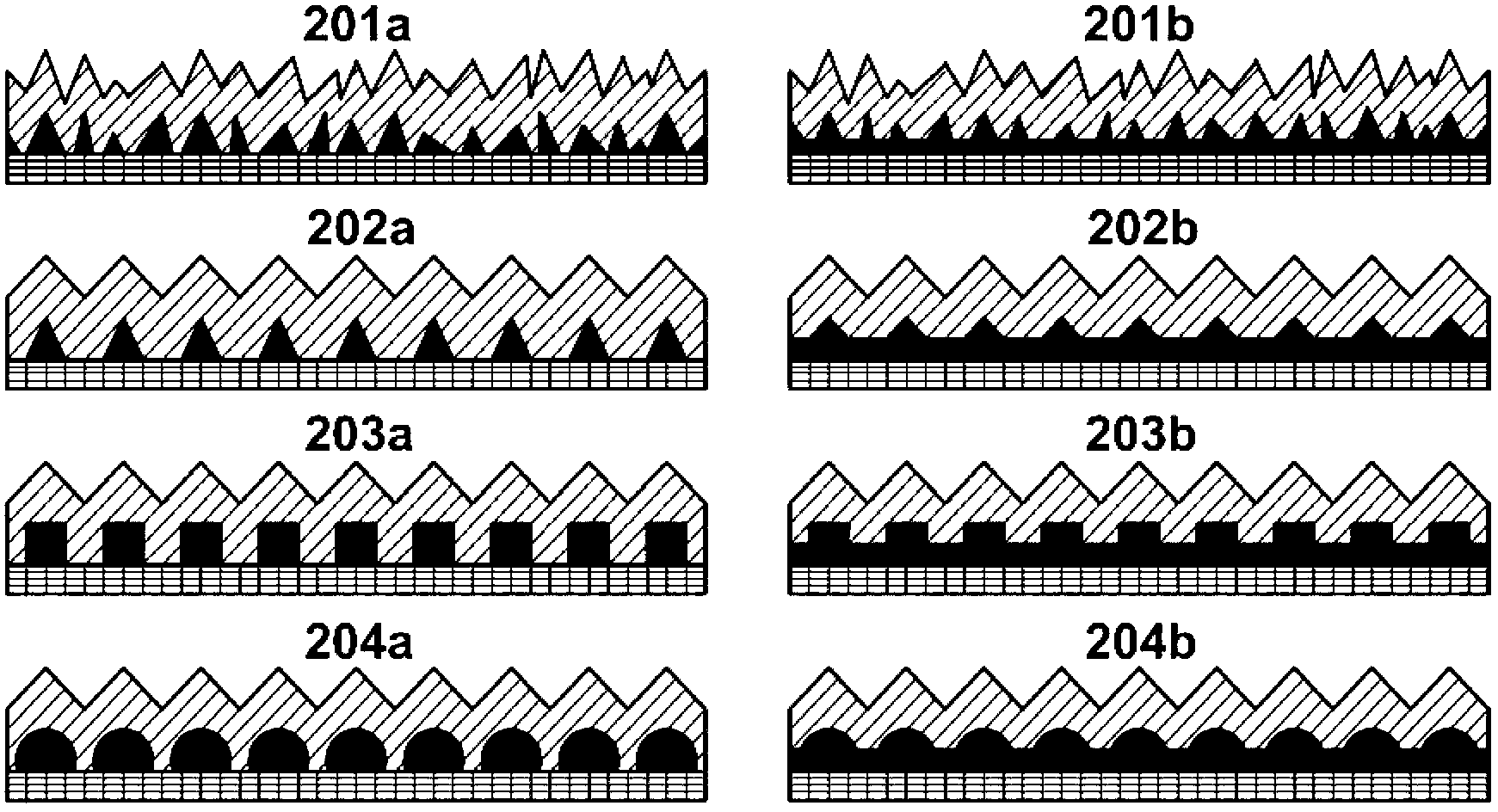
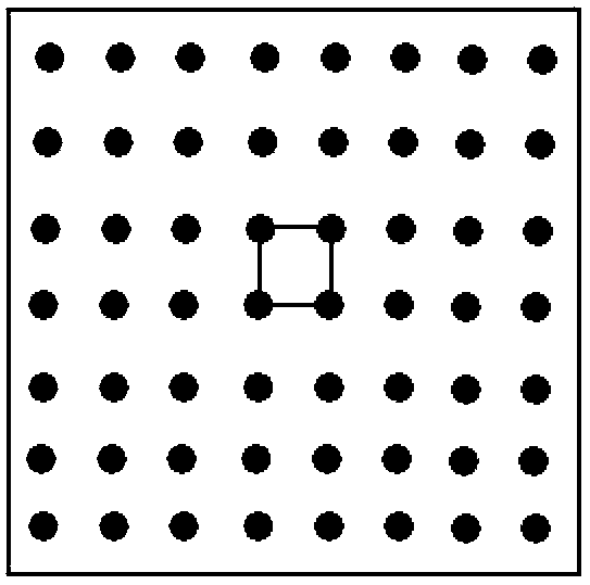
[0071] In this embodiment, the doped titanium oxide layer 105 and the indium tin oxide layer 106 are arranged periodically in space, thereby forming a two-dimensional photonic crystal structure, wherein the lattice constant is, for example, between 100 nanometers and 1 micrometer. The lattice type of the two-dimensional photonic crystal structure of the composite transparen...
PUM
| Property | Measurement | Unit |
|---|---|---|
| thickness | aaaaa | aaaaa |
| thickness | aaaaa | aaaaa |
| electrical resistance | aaaaa | aaaaa |
Abstract
Description
Claims
Application Information
 - R&D Engineer
- R&D Manager
- IP Professional
- Industry Leading Data Capabilities
- Powerful AI technology
- Patent DNA Extraction
Browse by: Latest US Patents, China's latest patents, Technical Efficacy Thesaurus, Application Domain, Technology Topic, Popular Technical Reports.
© 2024 PatSnap. All rights reserved.Legal|Privacy policy|Modern Slavery Act Transparency Statement|Sitemap|About US| Contact US: help@patsnap.com