Anti-dispersion structure and manufacturing process of electron multiplying charge-coupled device

A charge-coupled device and electron multiplying technology, applied in EMCCD structure and manufacturing, anti-dispersion channel and anti-dispersion barrier structure and manufacturing field, can solve the problems of imaging image dispersion, limited dynamic range, etc. Sensitivity, effect of high sensitivity response

Active Publication Date: 2015-10-28
EAST CHINA INST OF OPTOELECTRONICS INTEGRATEDDEVICE
View PDF8 Cites 0 Cited by
  • Summary
  • Abstract
  • Description
  • Claims
  • Application Information

AI Technical Summary

Problems solved by technology

[0006] In order to solve the problem of image dispersion in the EMCCD image sensor due to the limited dynamic range in the prior art under conditions such as strong light irradiation or relatively long light integration time, an anti-diffusion structure of EMCCD is proposed

Method used


Image

  • Anti-dispersion structure and manufacturing process of electron multiplying charge-coupled device
  • Anti-dispersion structure and manufacturing process of electron multiplying charge-coupled device
  • Anti-dispersion structure and manufacturing process of electron multiplying charge-coupled device

Examples


Embodiment Construction

[0025] The present invention will be further described below in conjunction with the accompanying drawings. The following examples are only used to illustrate the technical solution of the present invention more clearly, but not to limit the protection scope of the present invention.

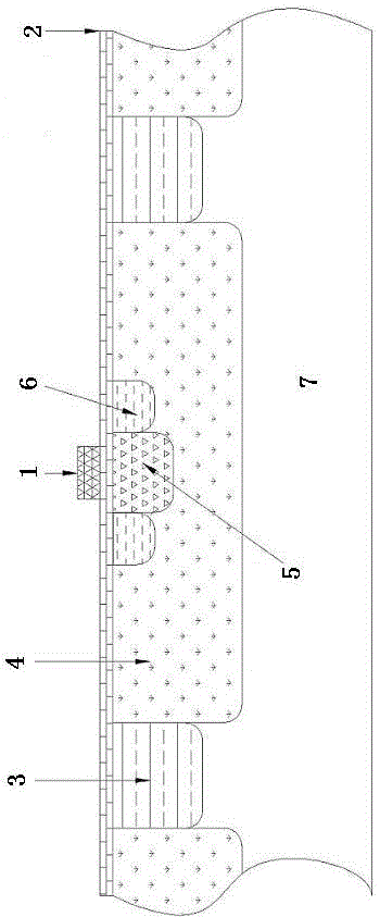
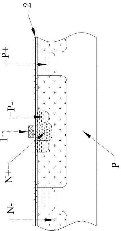
[0026] figure 1 It is a schematic diagram of an anti-diffusion structure realization approach of EMCCD, figure 2 It is a schematic cross-sectional view of an EMCCD imaging unit with an anti-diffusion structure. Various specific implementations can be made according to this figure. The EMCCD imaging unit with an anti-diffusion structure optimized by the method of the present invention is a multi-level semiconductor structure, mainly composed of electrodes 1 , an oxide layer 2, a trench resistance 3, a signal channel 4, an anti-diffusion channel 5, an anti-diffusion barrier 6, and a substrate 7.

[0027] In the figure, the substrate 7 is made of high-resistance P-type silicon (Si) material; the...


PUM


Abstract

The invention discloses an anti-dispersion structure of an electron multiplying charge-coupled device(EMCCD). According to the structure, an anti-dispersion channel is arranged in an imaging unit in an imaging area of the EMCCD; signal channels in the imaging unit in the imaging area of the EMCCD are arranged on two sides of the anti-dispersion channel. Excess photon-generated carriers generated due to glare irradiation or relatively over long light integrating time overflow to the anti-dispersion channel, and are converted into current to be released through the anti-dispersion channel, so as to inhibit dispersion phenomenon. According to the anti-dispersion structure, not only a low-light level imaging system based on the EMCCD has higher response sensitivity, but also the dynamic range of the low-light level imaging system taking the image sensor of the EMCCD as a core device is greatly broadened.

Description

technical field [0001] The invention relates to an EMCCD structure and a manufacturing method using Si integrated circuit technology, in particular to the structure and manufacturing method of an anti-diffusion channel and an anti-diffusion barrier, and belongs to the technical field of semiconductor integrated circuits. Background technique [0002] Electron multiplying charge-coupled device (EMCCD) is a brand-new all-solid-state low-light imaging device with high-speed readout capability. During the transfer process, impact ionization is used to achieve almost noise-free linear amplification of photogenerated charges, thereby realizing real-time fast dynamic detection and all-solid-state imaging of extremely weak light signals, which significantly improves the performance of low-light imaging devices. Reconnaissance, astronomical observation, biomedicine and other fields have great development potential and broad application prospects. [0003] The basic working process o...

Claims


Application Information

Patent Timeline
Patent Type & Authority Patents(China)
IPC IPC(8): H01L27/148
Inventor 刘庆飞邹继鑫戴放胡传菊于洪州
Owner EAST CHINA INST OF OPTOELECTRONICS INTEGRATEDDEVICE
Why Eureka
Try Eureka