Superconductivity nanometer single photon detecting chip and preparing process thereof

A single-photon detection and preparation technology, applied in the direction of sustainable manufacturing/processing, semiconductor device, final product manufacturing, etc., can solve the problems of reducing the working band and limiting the application of spectral analysis, etc., achieve a wide working band and increase the probability of photon absorption , a wide range of effects

Inactive Publication Date: 2013-10-23
NANJING UNIV
View PDF3 Cites 14 Cited by
  • Summary
  • Abstract
  • Description
  • Claims
  • Application Information

AI Technical Summary

Problems solved by technology

But at the same time, due to the wavelength selectivity of the superconducting resonant cavity, this method can only work in a specific band

Method used


Image

  • Superconductivity nanometer single photon detecting chip and preparing process thereof

Examples


Embodiment

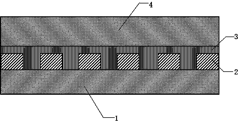
[0021] Example: A superconducting nanometer single-photon detection chip of the present invention comprises a substrate 1 , an active layer 2 , an insulating layer 3 and a photon absorption layer 4 .

[0022] The substrate 1 is the substrate of a common superconducting single-photon detection chip, and a MgO sheet or a Si sheet is used in this embodiment.

[0023] The active layer 2 is at least two superconducting nanowires arranged on the upper surface of the substrate 1 in a meandering structure. In this embodiment, the active layer 2 is a superconducting nanowire formed by exposure of a NbN film to an electron beam. The superconducting nanowire has a thickness of 4 nm and a width of 100 nm.

[0024] The photon absorbing layer 4 is a carbon nanotube layer with a thickness greater than 10 nanometers, and is arranged above the active layer 2;

[0025] The insulating layer 3 is an Al2O3 insulating layer, filled between at least two superconducting nanowires, and at the same ...


PUM

PropertyMeasurementUnit
Thicknessaaaaaaaaaa
Thicknessaaaaaaaaaa
Widthaaaaaaaaaa

Abstract

The invention discloses a superconductivity nanometer single photon detecting chip. The superconductivity nanometer single photon detecting chip comprises a substrate, an active layer, insulating layers and a photon absorbed layer. The active layer comprises at least two superconductivity nanometer wires, and is arranged on the upper surface of the substrate in a zigzag structure mode. The photon absorbed layer is a carbon nanometer tube layer, and is arranged on the active layer. The portion between the two superconductivity nanometer wires is filled with the insulating layer, and the portion between the superconductivity nanometer wires and the photon absorbed layer is filled with the insulating layers. The invention further provides a preparing process of the superconductivity nanometer single photon detecting chip. The preparing process greatly improves the photon absorbing probability of a detector chip and improves the absorbable photon wave band to be the ultraviolet-visible light-infrared wave band, so that the system efficiency of a detector is improved, and the superconductivity nanometer single photon detecting chip is high in efficiency, and wide in working wave band and in application range.

Description

technical field [0001] The invention relates to a detection chip, in particular to a superconducting nanometer single-photon detection chip. Background technique [0002] Photon is the fundamental particle that transmits electromagnetic interaction, and it is a kind of gauge boson. Photon is the carrier of electromagnetic radiation, and photon is considered as the mediator of electromagnetic interaction in quantum field theory. Compared to most elementary particles, photons have zero rest mass, which means they travel at the speed of light in a vacuum. Like other quanta, photons have wave-particle duality: photons can exhibit properties such as refraction, interference, and diffraction of classical waves; while the particle nature of photons shows that when interacting with matter, they are not like classical particles that can transmit any value of energy, photons can only transfer quantized energy. For visible light, the energy carried by a single photon is about 4×10⁻¹...

Claims


Application Information

Patent Timeline
IPC IPC(8): H01L31/09H01L31/0256H01L31/18
CPCY02P70/50
Inventor 张蜡宝徐睿莹康琳陈健吴培亨
Owner NANJING UNIV
Why Eureka
Try Eureka