Back passivation solar cell and manufacturing method thereof

The technology of a solar cell and its manufacturing method, which is applied in the field of solar cells, can solve the problems that the conversion efficiency of back passivated solar cells needs to be improved, and achieve the effects of reducing carrier recombination, improving conversion efficiency, and reducing contact area

Inactive Publication Date: 2013-10-23
YINGLI GRP +2
View PDF2 Cites 6 Cited by
  • Summary
  • Abstract
  • Description
  • Claims
  • Application Information

AI Technical Summary

Problems solved by technology

[0004] However, it is found in the actual production process that the conversion efficiency of conventional back passivated solar cells needs to be improved.

Method used


Image

  • Back passivation solar cell and manufacturing method thereof
  • Back passivation solar cell and manufacturing method thereof
  • Back passivation solar cell and manufacturing method thereof

Examples


Embodiment 1

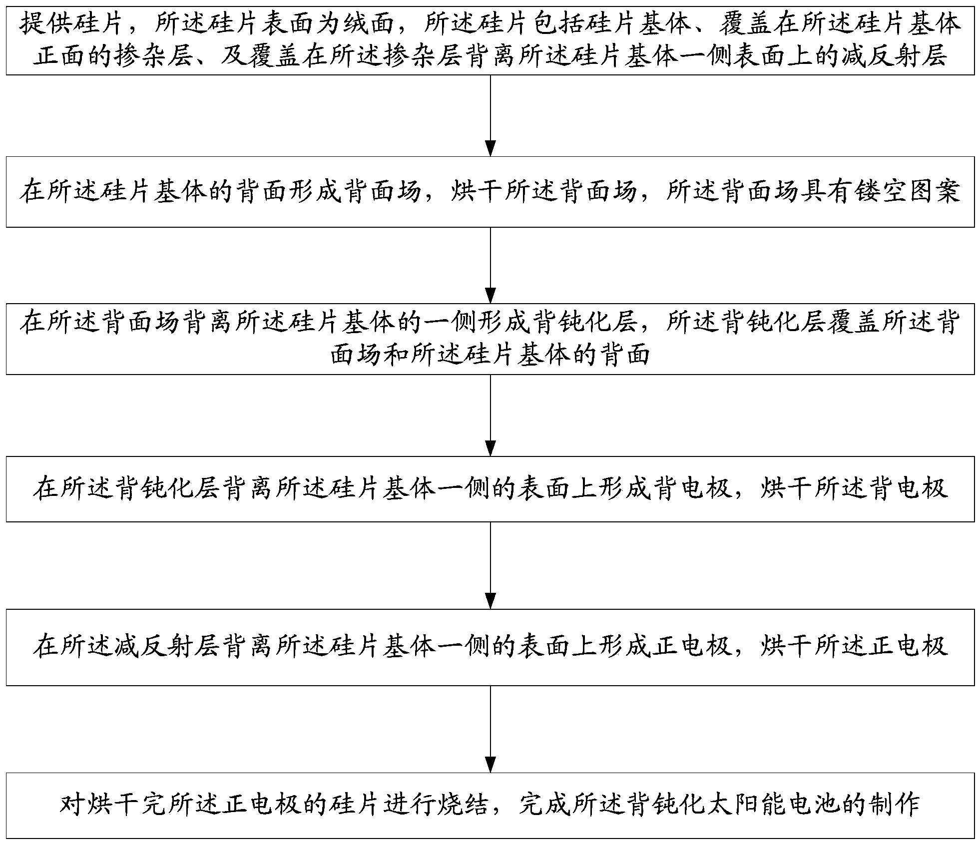
[0053] This embodiment provides a method for making a back passivated solar cell, such as figure 2 As shown, the method includes:

[0054] providing a silicon wafer, the silicon wafer comprising a silicon wafer substrate, a doped layer covering the front surface of the silicon wafer substrate, and an anti-reflection layer covering the surface of the doped layer facing away from the silicon wafer substrate;

[0055] After removing the surface damage layer and preparing the textured surface of the silicon wafer, one side is diffused to form a doped layer, and the interface between the doped layer and the silicon wafer substrate forms a PN junction. Then etch the edge of the silicon wafer to remove the PN junction on the edge side of the silicon wafer, then remove the glass layer formed on the front of the silicon wafer during the diffusion process, and then PECVD (Plasma Enhanced Chemical Vapor Deposition, plasma enhanced chemical vapor deposition) on the front of the silicon w...

Embodiment 2

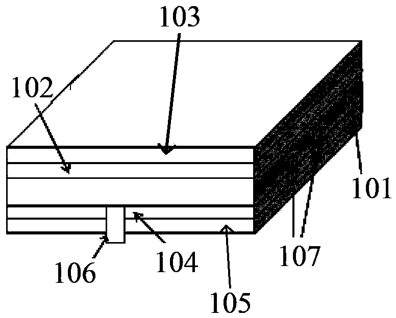
[0080] Based on the first embodiment, this embodiment provides a back passivated solar cell, such as Figure 5 As shown, the back passivated solar cell includes:

[0081] A silicon wafer substrate 501, a doped layer 502 covering the front surface of the silicon wafer substrate 501, and an anti-reflection layer 503 covering the surface of the doped layer 502 facing away from the silicon wafer substrate 501;

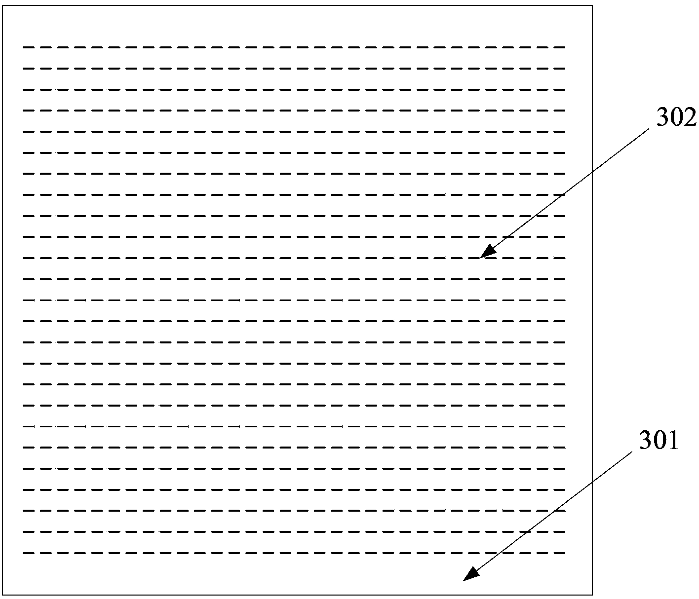
[0082] A back field 504 located on the back side of the silicon wafer substrate 501, the back field 504 has a hollow pattern;

[0083] A back passivation layer 505 located on the side of the back surface field 504 away from the silicon substrate 501, the back passivation layer 505 covering the back surface field 504 and the back surface of the silicon substrate 501;

[0084] a back electrode (not shown in the figure) located on the surface of the back passivation layer 505 facing away from the silicon substrate 501;

[0085] A positive electrode (not shown in the figure)...


PUM


Abstract

The invention provides a manufacturing method of a back passivation solar cell. After an antireflection film is prepared on a silicon wafer, a back surface field with hollowed-out patterns is firstly formed, then a back passivation layer is formed, and afterwards, a positive electrode is formed. Through forming the back surface field before the back passivation layer, the step of laser grooving is saved, so that damage to the silicon wafer caused by laser grooving is avoided; and since the back surface field is in a hollowed-out structure, the contact area of the back surface field with the back passivation layer is reduced, so that the erosion degree of the back surface field over the back passivation layer is lightened, the back passivation layer can well play a passivation effect, recombination of current carriers on the back surface of the cell is reduced, and finally, the conversion efficiency of the back passivation solar cell can be improved. Since the step of laser grooving is not needed, the production process is simplified; since the back surface field is in the hollowed-out structure, the use amount of materials needed for manufacturing the back surface field is reduced, so that the production cost is lowered; and by using the back surface field in the hollowed-out structure, stress bending caused by differences of expansion coefficients of silicon and aluminum can be reduced, so that cell breakage caused by cell bending is reduced.

Description

technical field [0001] The invention relates to the technical field of solar cells, more specifically, to a back passivated solar cell and a manufacturing method thereof. Background technique [0002] A solar cell is a semiconductor device that converts the sun's light energy directly into electrical energy. Because it is a green product, does not cause environmental pollution, and uses renewable resources, solar cells have broad prospects for development in today's energy shortage situation. [0003] Preparing a passivation layer on the back of the silicon wafer to form a back passivation battery can reduce the recombination of carriers on the back of the battery, increase the life of the carriers, and improve the conversion efficiency of the battery. Usually the production process of back passivation solar cell is: remove the surface damage layer and prepare suede surface-diffusion to make PN junction-edge etching and de-glass layer-preparation of anti-reflection layer-pr...

Claims


Application Information

Patent Timeline
Patent Type & Authority Applications(China)
IPC IPC(8): H01L31/18H01L31/068H01L31/0224
CPCY02E10/50H01L31/022425H01L31/068H01L31/1804Y02E10/547Y02P70/50
Inventor 徐卓杨学良杨德成赵文超李高非胡志岩熊景峰
Owner YINGLI GRP
Why Eureka
Try Eureka