Silicon nitride film deposition method, organic electronic device manufacturing method, and silicon nitride film deposition device
A technology of organic electronic devices and silicon nitride films, which is applied in semiconductor/solid-state device manufacturing, electric solid-state devices, electrical components, etc., can solve problems such as shortened life of organic EL components, and achieve the effect of improving controllability
- Summary
- Abstract
- Description
- Claims
- Application Information
AI Technical Summary
Problems solved by technology
Method used
Image

Examples
Embodiment Construction
[0031] Hereinafter, embodiments of the present invention will be described with reference to the drawings. However, in this specification and the drawings, the same reference numerals are attached to constituent elements having substantially the same functions, and repeated descriptions are omitted.
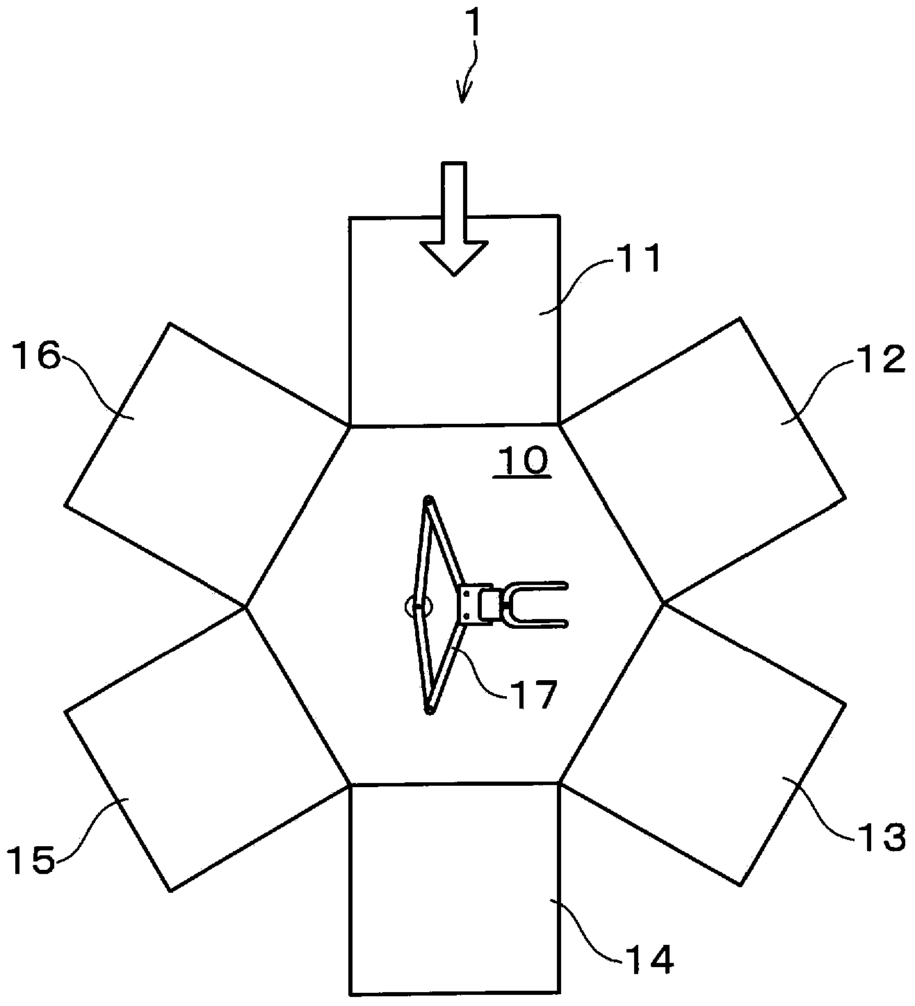
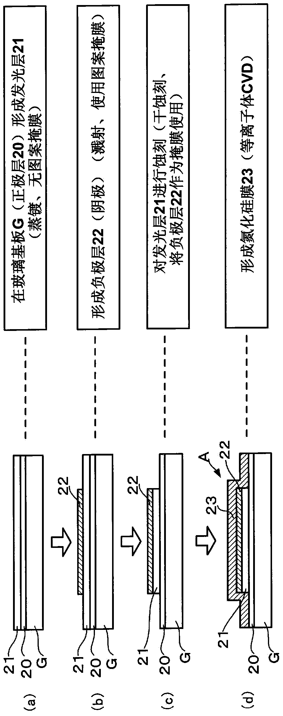
[0032] First, a method for manufacturing an organic electronic device according to an embodiment of the present invention will be described together with a substrate processing system for implementing the method. figure 1 It is an explanatory diagram showing a schematic configuration of the substrate processing system 1 . figure 2 It is an explanatory drawing showing the manufacturing process of an organic EL device. In addition, in this embodiment mode, the case where an organic EL device is manufactured as an organic electronic device is demonstrated.
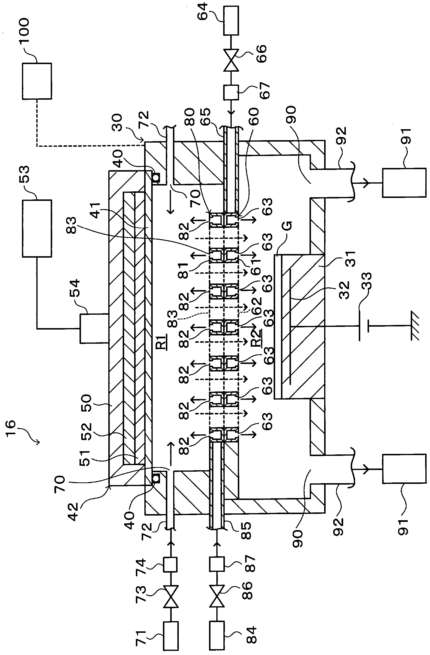
[0033] Such as figure 1 As shown, a cluster substrate processing system 1 has a transfer chamber 10 . The transport chamb...
PUM
 Abstract
Description
Claims
Application Information
PatSnap Eureka turns technology decisions into work you can execute. Powered by our Innovation Knowledge Graph, it runs expert workflows across engineering, life sciences, materials and intellectual property. Get your review-ready output in minutes.


