Method for manufacturing plane solid state supercapacitor

A supercapacitor, solid-state technology, applied in semiconductor/solid-state device manufacturing, hybrid/electric double-layer capacitor manufacturing, circuits, etc., can solve the problems of high cost, immaturity, and incompatibility of standard semiconductor device manufacturing processes, and achieve low cost , suitable for mass production

Inactive Publication Date: 2013-11-27
NANJING UNIV
View PDF6 Cites 7 Cited by
  • Summary
  • Abstract
  • Description
  • Claims
  • Application Information

AI Technical Summary

Problems solved by technology

[0006]Technical problems to be solved: Aiming at the problems of high cost, immaturity, and incompatibility with standard semiconductor device manufacturing processes in the above supercapacitor research, a Low-cost, energy-saving and environmentally friendly, mass-producible planar solid-state supercapacitors compatible with standard semiconductor fabrication processes

Method used


Image

  • Method for manufacturing plane solid state supercapacitor
  • Method for manufacturing plane solid state supercapacitor
  • Method for manufacturing plane solid state supercapacitor

Examples


Embodiment 1

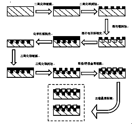
[0026] The present invention is a kind of preparation method of planar solid supercapacitor, comprises the following steps:

[0027] (1) Pretreatment of the surface of the silicon wafer: immerse the surface of the silicon wafer with 3wt% hydrogen fluoride solution for 60 seconds, and then wash it with distilled water.

[0028] (2) The chemical vapor deposition method is used for silicon dioxide coating, the coating temperature is 480°C, and the coating thickness is 0.45 microns.

[0029] (3) Perform photolithography on the silicon dioxide protective layer, including: 1) Cleaning: cleaning the surface of the silicon wafer with distilled water; 2) Coating photoresist and pre-baking at 220°C; 3) Aligning and exposing on a photolithography machine, Development; 4) Post-baking at 380°C; 5) Use isopropanol solution to dissolve the photoresist on the developed part, and then clean the wafer surface with distilled water; 6) Use 3wt% HF solution to etch the part not covered by photores...

Embodiment 2

[0043] A preparation method of a planar solid supercapacitor of the present invention comprises the following steps:

[0044] (1) Pretreatment of the surface of the silicon wafer: immerse the surface of the silicon wafer with 3wt% hydrogen fluoride solution for 60 seconds, and then wash it with distilled water.

[0045] (2) The chemical vapor deposition method is used for silicon dioxide coating, the coating temperature is 300°C, and the coating thickness is 0.1 micron.

[0046](3) Photolithography of the silicon dioxide protective layer, including: 1) Cleaning: cleaning the surface of the silicon wafer with distilled water; 2) Coating photoresist and pre-baking at 220°C; 3) Alignment, exposure, and development on a photolithography machine ; 4) Post-baking at 380°C; 5) Use isopropanol solution to dissolve the photoresist on the developed part, and then clean the wafer surface with distilled water; 6) Use 3wt% HF solution to etch the parts not covered by photoresist Silicon d...

Embodiment 3

[0060] A preparation method of a planar solid supercapacitor of the present invention comprises the following steps:

[0061] (1) Pretreatment of the surface of the silicon wafer: immerse the surface of the silicon wafer with 3wt% hydrogen fluoride solution for 60 seconds, and then wash it with distilled water.

[0062] (2) The chemical vapor deposition method is used for silicon dioxide coating, the coating temperature is 580°C, and the coating thickness is 0.55 microns.

[0063] (3) Photolithography of the silicon dioxide protective layer, including: 1) Cleaning: cleaning the surface of the silicon wafer with distilled water; 2) Coating photoresist and pre-baking at 250°C; 3) Alignment, exposure, and development on a photolithography machine ;4) Post-baking at 420°C; 5) Use isopropanol solution to dissolve the photoresist on the developed part, and then clean the wafer surface with distilled water; 6) Use 3wt% HF solution to etch the parts not covered by photoresist Silicon...


PUM

PropertyMeasurementUnit
thicknessaaaaaaaaaa
thicknessaaaaaaaaaa
thicknessaaaaaaaaaa

Abstract

The invention relates to a method for manufacturing a plane solid state supercapacitor. The plane solid state supercapacitor is manufactured on a standard silicon wafer, standard methods, such as the chemical vapor deposition method, the physical vapor deposition method, the groove etching method, the chemical-mechanical polishing method and the three-dimensional method based on silicon through holes, in the semiconductor device manufacturing process are used, a composition composed of one kind or several kinds of SiO2, Al2O3 and HfO2 or Ba(Sr)TiO3 serves as a core, and the plane solid state supercapacitor is compatible with a standard semiconductor device. The plane solid state supercapacitor has the advantages of being low in cost, saving energy and being environmentally friendly and suitable for mass manufacturing.

Description

technical field [0001] The present invention relates to a kind of preparation method of supercapacitor, particularly relate to a kind of SiO 2 、Al 2 o 3 , HfO 2 or Ba(Sr)TiO 3 A method for preparing a planar solid-state supercapacitor whose core is a composition composed of one or several compositions, and which is compatible with standard semiconductor device preparation processes. Background technique [0002] Solid-state supercapacitors have become one of the mainstream development directions of new green energy storage technologies. According to the analysis of the 2011 annual report of Freedonia Research Group, an international authoritative organization, in 2011, various planar solid-state supercapacitor products have occupied a market of about 600 million US dollars. In the past few years, the booming green energy industry in the world has used more and more solid-state supercapacitors, and the quality requirements have become higher and higher. With the rapid d...

Claims


Application Information

Patent Timeline
Patent Type & Authority Applications(China)
IPC IPC(8): H01G11/84H01L21/02
CPCY02E60/13
Inventor 史方王晓晨周洁孔令宇潘毅虞磊韩建林
Owner NANJING UNIV
Why Eureka
Try Eureka