Beam shaping device for semiconductor laser

A beam shaping and laser technology, applied in optics, instruments, optical components, etc., can solve the problems of large power value and poor beam quality, etc., and achieve the effect of improving comprehensive beam quality and good beam quality.

Inactive Publication Date: 2013-12-04
JIANGSU SKYERALASER TECH
View PDF7 Cites 4 Cited by
  • Summary
  • Abstract
  • Description
  • Claims
  • Application Information

AI Technical Summary

Problems solved by technology

Although the current semiconductor beam combining technology can combine the output beams of multiple semiconductor lasers into one, but due to the huge differe

Method used


Image

  • Beam shaping device for semiconductor laser
  • Beam shaping device for semiconductor laser

Examples


Embodiment 1

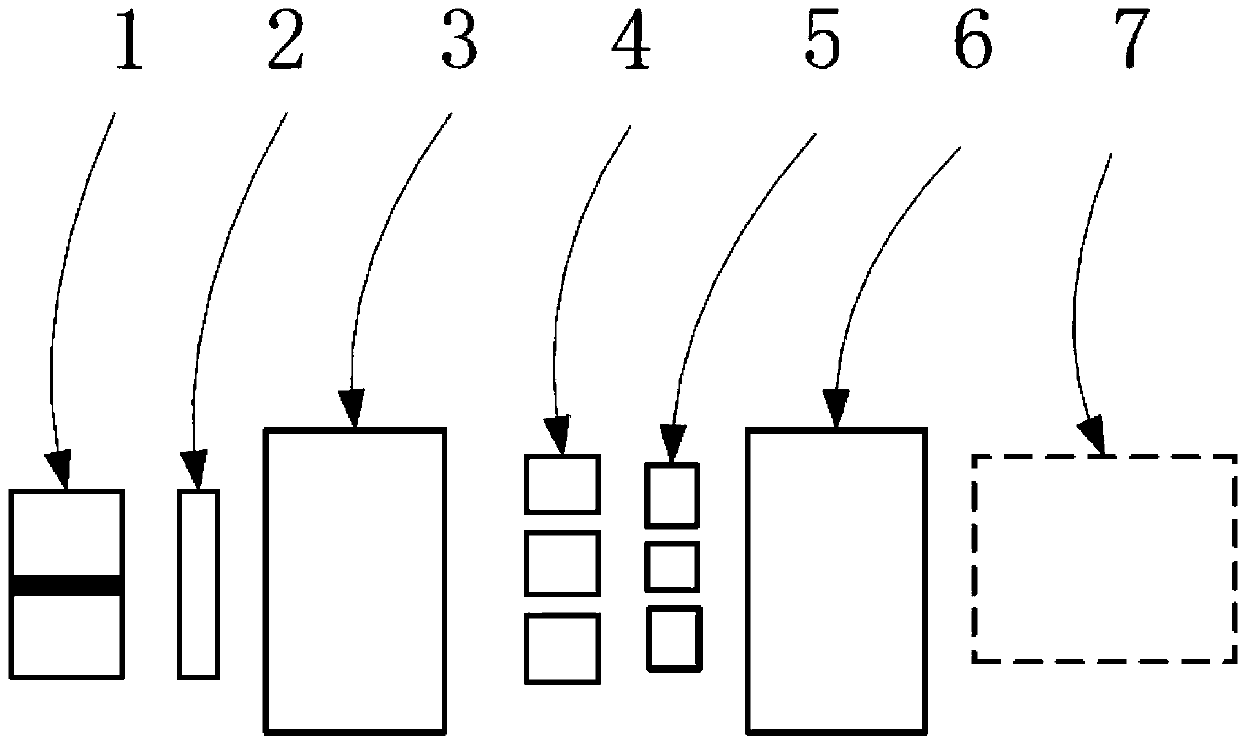
[0023] The device of the present invention is as figure 1 shown.

[0024] Below in conjunction with accompanying drawing, preferred specific embodiment of the present invention is described:

[0025] A semiconductor laser die 1 with 975nm, output power of 10W, output bar width Lx=150 microns, and optical mode field thickness Ly=1 micron is used. The divergence angle of the fast axis (y axis) is 70°, and the slow axis (x axis) The divergence angle is 18°, and it is mounted on an aluminum nitride transition heat sink and a copper heat sink. The original BPP of the semiconductor laser die 1 is 0.34 mm.mrad on the y-axis and 9.8 mm.mrad on the x-slow axis. Use the first fast-axis collimating lens 2 to partially collimate the fast axis of the semiconductor laser tube core 1, so that the image of the light-emitting surface of the tube core basically overlaps in the fast-axis direction and the slow-axis direction to form a unified image. The y divergence angle is 30°, the x diverg...


PUM


Abstract

A beam shaping device for a semiconductor laser is characterized in that (i) a light-emitting area of a semiconductor laser tube core is linearly amplified by an optical amplifying element, (ii) the light-emitting area is sectioned, each section is optically transformed in a 90-degree rotating manner by a 90-degree optical rotating element, (iii) spatial translation is performed on each section by an optical translation element, so that the sections are closer, and gaps among the sections are narrowed, (iv) an image in the light-emitting area is properly linearly reduced by an optical reduction element, so that a linear size and a divergence angle adapting to output are formed. By the aid of the device, the BPP (beam parameter product) of an output beam of the semiconductor laser is decreased, beam quality is improved, and a powerful technological path is provided for manufacture of a high-power semiconductor pump laser and a high-power direct semiconductor laser system.

Description

technical field [0001] The invention relates to a beam shaping device, in particular to a beam shaping device of a semiconductor laser. Background technique [0002] With the application of semiconductor high-power laser technology in fiber laser pumping and direct semiconductor lasers, semiconductor lasers are required to output higher power and have better beam quality. In a high-power fiber laser system, the greater the power of the semiconductor pump laser, the fewer the number of branches of the fiber combiner required, and the simpler the system structure, it is easier to manufacture and maintain. In high-power direct semiconductor lasers, it is necessary to combine the beams of as many semiconductor lasers as possible, and at the same time require the beam quality to be as good as possible. But the current difficulty lies in the fact that the slow axis (horizontal) direction of the light emitting region of the semiconductor laser is relatively wide, on the order of h...

Claims


Application Information

Patent Timeline
IPC IPC(8): G02B27/09
Inventor 李丰黄伟谈根林
Owner JIANGSU SKYERALASER TECH
Why Eureka
Try Eureka