BCD integrated device and manufacturing method of BCD integrated device

A technology of integrated devices and oxide semiconductors, which can be used in semiconductor/solid-state device manufacturing, semiconductor devices, electric solid-state devices, etc., and can solve the problems of limited application scope, high cost of buried layer and epitaxial layer process

Active Publication Date: 2013-12-04
深圳市深超科技投资有限公司
View PDF4 Cites 3 Cited by
  • Summary
  • Abstract
  • Description
  • Claims
  • Application Information

AI Technical Summary

Problems solved by technology

[0005] The embodiment of the present invention provides a BCD integrated device and its manufacturing method, which is used to solve the problem existing in the prior art that the process cost of making the buried layer and the epitaxial layer is very high, thereby limiting its application range

Method used


Image

  • BCD integrated device and manufacturing method of BCD integrated device
  • BCD integrated device and manufacturing method of BCD integrated device
  • BCD integrated device and manufacturing method of BCD integrated device

Examples


Embodiment Construction

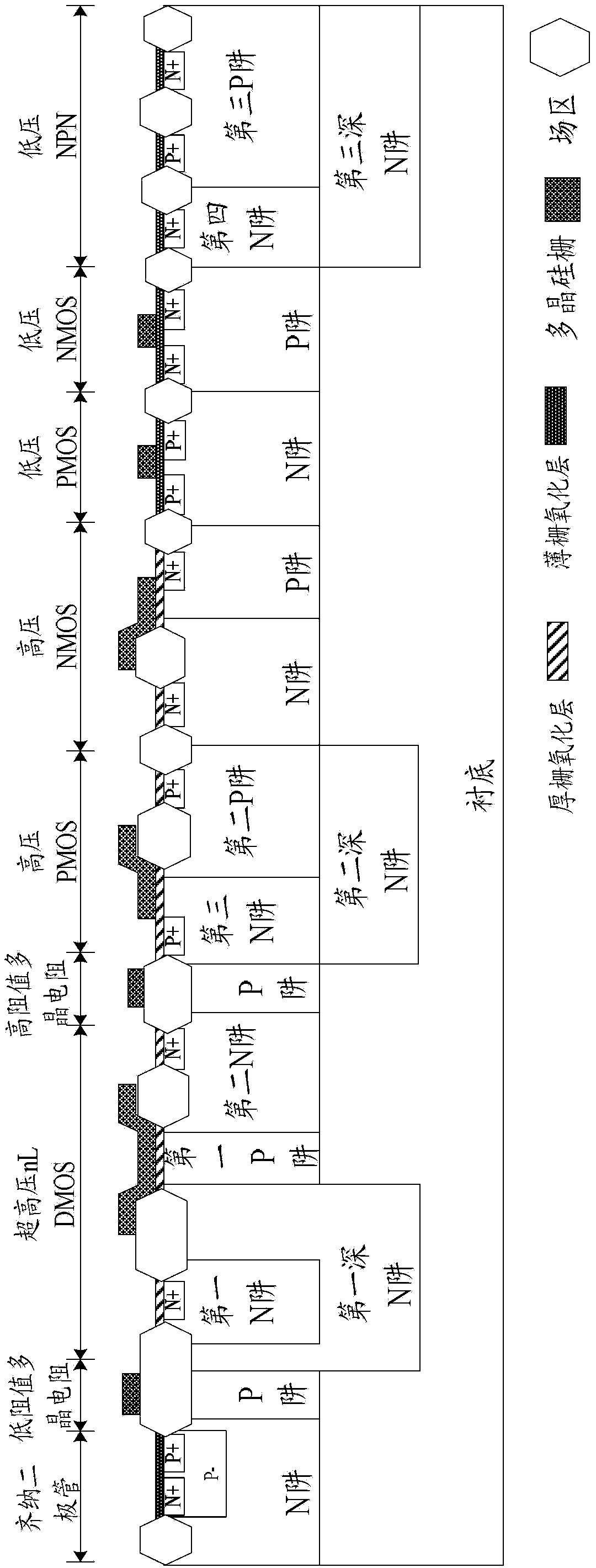
[0028] The BCD integrated device introduced in the embodiment of the present invention adopts a non-epitaxial process to form an ultra-high voltage nLDMOS, a high voltage PMOS and a low voltage NPN in a P-type single crystal substrate. Since the ultra-high voltage nLDMOS, high voltage PMOS and low voltage NPN are directly fabricated in the substrate, no epitaxial layer in the traditional process is required, thereby reducing the manufacturing cost, improving the cost performance, expanding its application range, and making up for the shortcomings of the existing technology .

[0029] The embodiments of the present invention will be further described in detail below in conjunction with the accompanying drawings.

[0030] In practice, in order to reduce manufacturing costs, non-epitaxial processes can be used to fabricate devices in the substrate; in the embodiment of the present invention, ultra-high voltage nLDMOS, high-voltage PMOS and low-voltage NPN are located in the subst...


PUM


Abstract

The invention relates to the field of semiconductor integrated circuit manufacturing, in particular to a BCD integrated device and a manufacturing method of the BCD integrated device so as to solve the problem that in the prior art, due to the fact that the process cost for manufacturing a buried layer and an epitaxial layer is very high, the application range of the BCD integrated device is limited. According to the embodiment, the manufacturing method of the BCD integrated device refers to a substrate, an ultrahigh voltage nLDMOS, a high voltage PMOS and a low voltage NPN, wherein the ultrahigh voltage nLDMOS, the high voltage PMOS and the low voltage NPN are located in the substrate. The ultrahigh voltage nLDMOS, the high voltage PMOS and the low voltage NPN are directly manufactured in the substrate, therefore, the epitaxial layer in the prior art is not needed, the manufacturing cost is lowered, the cost performance is improved, the application range of the BCD integrated device is broadened, and the shortcomings in the prior art are overcome.

Description

technical field [0001] The invention relates to the field of semiconductor integrated circuit manufacturing, in particular to a BCD integrated device and a manufacturing method thereof. Background technique [0002] BCD (Bipolar Transistor - Complementary Metal Oxide Semiconductor Field Effect Transistor - Double Diffused Metal Oxide Semiconductor Field Effect Transistor, Bipolar-CMOS-DMOS) is a bipolar transistor, CMOS (Complementary Metal Oxide Semiconductor, Complementary Metal Oxide Semiconductor) and DMOS (Double-diffused MOSFET, Double-diffused Metal Oxide Semiconductor Field Effect Transistor) integrated circuit technology, BCD combines high transconductance of bipolar devices, strong load drive capability, and CMOS integration The advantages of high precision and low power consumption. More importantly, it integrates DMOS power devices. DMOS can work in switch mode, with extremely low power consumption, and can deliver high power to the load without expensive packag...

Claims


Application Information

Patent Timeline
Patent Type & Authority Applications(China)
IPC IPC(8): H01L27/06H01L21/8249
Inventor 潘光燃石金成
Owner 深圳市深超科技投资有限公司
Why Eureka
Try Eureka