Semiconductor device and manufacturing method thereof

A device manufacturing method and semiconductor technology, applied in the direction of semiconductor/solid-state device manufacturing, semiconductor devices, electrical components, etc., can solve the problem of reducing driving ability, etc., and achieve the effects of preventing stress reduction, eliminating voids, and eliminating STI edge effects

Active Publication Date: 2013-12-04
INST OF MICROELECTRONICS CHINESE ACAD OF SCI
View PDF6 Cites 7 Cited by
  • Summary
  • Abstract
  • Description
  • Claims
  • Application Information

AI Technical Summary

Problems solved by technology

Similar to PMOS, SiC will also become thinner at the STI edge of NMOS, reducing the drive capability

Method used


Image

  • Semiconductor device and manufacturing method thereof
  • Semiconductor device and manufacturing method thereof
  • Semiconductor device and manufacturing method thereof

Examples


Embodiment Construction

[0034] The features and technical effects of the technical solution of the present invention will be described in detail below with reference to the accompanying drawings and in combination with exemplary embodiments. It should be pointed out that similar reference numerals represent similar structures, and the terms "first", "second", "upper", "lower", "thick", "thin" and the like used in this application can be used for Modification of various device structures and method steps. These modifications do not imply a spatial, sequential or hierarchical relationship of the modified device structures and method steps thereof unless specifically stated.

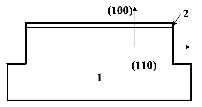
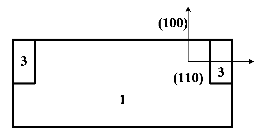
[0035] 7 to 13 show schematic cross-sectional views of epitaxial growth of SiGe on source and drain regions according to the present invention.

[0036]First, as shown in FIG. 7, the substrate 10 is etched by conventional mask exposure to form a shallow trench surrounding an opening region (or active region), and then pad oxide i...


PUM


Abstract

The invention provides a semiconductor device which comprises a substrate, a shallow trench isolation, a channel region, a gate stack and source-drain regions. The STI is embedded into the substrate and provided with at least one open region; the channel region is arranged in the open region; the gate stack comprises a gate medium layer and a gate electrode layer, and is located above the channel region; the source-drain regions are arranged on two sides of the channel region, and each source-drain region comprises a stress layer used for providing strain for the channel region. A packing layer is arranged between the STI and each stress layer and serves as a crystal seed layer of the stress layer; a packing layer and a cushion oxidation layer are arranged between the substrate and the STI. According to the semiconductor device, due to the fact that the packing layer is inserted between the STI and the stress layer of each source-drain region and serves as the crystal seed layer or a nucleating layer for epitaxial growth, the STI fringe effect in source-drain strain engineering is eliminated, a gap between the STI and the stress layer of each source-drain region is also eliminated, reduction of stress of the source-drain strain on channels is prevented, the carrier mobility of MOS devices is improved, and therefore the drive capability of the devices is improved.

Description

technical field [0001] The invention relates to the field of semiconductor devices, in particular to a semiconductor device structure with an improved epitaxial edge and a manufacturing method thereof. Background technique [0002] The current method of reducing cost by reducing the feature size alone has encountered a bottleneck, especially when the feature size drops below 150nm, many physical parameters cannot be scaled, such as silicon band gap Eg, Fermi potential The interface state and oxide layer charge Qox, thermoelectric potential Vt and self-built potential of pn junction, etc., will affect the performance of scaled down devices. [0003] In order to further improve device performance, stress is introduced into the MOSFET channel region to improve carrier mobility. For example, on a wafer with a crystal plane of (100), the crystal orientation of the channel region is <110>. In PMOS, the stress along the longitudinal axis (along the source-drain direction) n...

Claims


Application Information

Patent Timeline
Patent Type & Authority Applications(China)
IPC IPC(8): H01L29/06H01L29/78H01L21/336
CPCH01L29/7848H01L29/66636H01L29/06H01L29/78H01L21/76224
Inventor 王桂磊崔虎山赵超
Owner INST OF MICROELECTRONICS CHINESE ACAD OF SCI
Why Eureka
Try Eureka