Input voltage sampling compensating circuit

A compensation circuit and input voltage technology, applied in the field of compensation circuits, can solve the problems of large temperature coefficient and affect sampling accuracy, and achieve the effects of good compensation effect, low power consumption, and simple power supply peripheral circuits

Active Publication Date: 2013-12-04
MORNSUN GUANGZHOU SCI & TECH
View PDF5 Cites 25 Cited by
  • Summary
  • Abstract
  • Description
  • Claims
  • Application Information

AI Technical Summary

Problems solved by technology

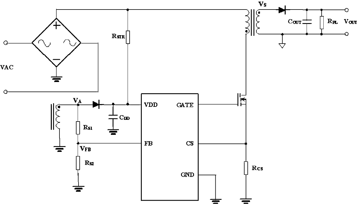
However, the working voltage of the chip is low, that is, |V A | When smaller, V BE cannot be ignored, and V BE The temperature coefficient is large, which directly affects the sampling accuracy
And because V BE0 voltage drop and the presence of ESD resistor Resd, if the voltage drop of ESD diode D1 V D1 If

Method used


Image

  • Input voltage sampling compensating circuit
  • Input voltage sampling compensating circuit
  • Input voltage sampling compensating circuit

Examples


Embodiment 1

[0041] A high-precision input voltage sampling circuit with self-compensation, comprising a first resistor R1, a second resistor R2, an operational amplifier amp, a bias resistor R2, a first logic NOT gate not1, and a first N-channel MOS transistor MN1 ,, the first transistor Q1, the second transistor Q2, the first P-channel MOS transistor MP1, the second P-channel MOS transistor MP2, the third P-channel MOS transistor MP3, and the P-type MOS transistor MP1, MP2 and MP3 form a feed-forward current mirror current mirror.

[0042] Such as Figure 7 Shown is the circuit diagram of the first embodiment of the present invention: VCC is the low-voltage power supply terminal of the chip; the output terminal of the bias current source Iref, the first port of the resistor R1, the drain terminal of the PMOS transistor MP2, and the positive input of the operational amplifier The terminals are connected together to form the first node; the second port of the resistor R1, the collector an...

Embodiment 2

[0053] Such as Figure 8 Shown is the circuit diagram of the second embodiment of the present invention: VCC is the low-voltage power supply terminal of the chip; the output terminal of the bias current source Iref, the first port of the resistor R1, the drain terminal of the PMOS transistor MP2, and the positive input of the operational amplifier The terminals are connected together to form the first node; the second port of the resistor R1, the collector and the base of the transistor Q1 are connected together to form the second node; the output terminal of the operational amplifier, the input negative terminal of the operational amplifier, and the input of the transmission gate T1 The ports are connected together to form the ③ node; the output terminal of the logic NOT gate not1, the input terminal of the logic NOT gate not2, the gate of the N-channel MOS transistor MN1, and the selection input negative terminal of the transmission gate T1 are connected together to form the ...

Embodiment 3

[0056] Such as Figure 9 As shown, compared with the second embodiment, the difference is that the sources and substrates of the current mirror MOS transistors MP1, MP2, and MP3 are all connected to the external high-voltage power supply VDD of the chip instead of the internal low-voltage power supply VCC of the chip. The advantage of doing this is: in some applications, a relatively large feed-forward current is required, that is, the current flowing through MP1, MP2, and MP3 is relatively large, and the internal power supply VCC is generated by the step-down of the external power supply VDD. The drive capability is limited, and this creates large power supply noise on the internal power supply. If the current of the current mirror is all absorbed from the external power supply VDD, the noise generated in the internal power supply VCC is very small.


PUM


Abstract

An input voltage sampling compensating circuit comprises a first resistor for electro-static discharge (ESD) resistor voltage drop compensating, a zero potential temperature compensating audion, an operational amplifier, a second resistor for biasing or current limiting, a clamping audion, a feed-forward current image current mirror and a sampling trigger port. An emitter electrode of the compensating audion is grounded, a base electrode and a collector electrode are connected and then connected with one end of the first resistor; the other end of the first resistor is connected with a working power supply and the in-phase input end of the operational amplifier respectively, the output end of the operational amplifier is connected with a base electrode of the clamping audion through the second resistor, the base electrode is connected with the output end of the sampling trigger port, an emitter electrode of the clamping audion is used for being connected with the external ESD resistor, and a collector electrode is connected with the input end of the feed-forward current image current mirror; the power end of the feed-forward current image current mirror is connected with the working power supply, and the compensating current output end of the feed-forward current image current mirror is connected with the other end of the first resistor. The circuit is capable of compensating for the voltage drop on the ESD resistor, provided with a temperature self-compensating function and free of influences from the ESD resistor and the temperature.

Description

technical field [0001] The invention relates to a compensation circuit, in particular to a compensation circuit for input voltage sampling. Background technique [0002] Because the flyback converter has the excellent characteristics of simple structure and low cost, it has become the first choice of many power supply engineers. However, most flyback converters are controlled by secondary side feedback, that is, the output voltage is fed back to the primary side of the converter through the transconductance amplifier formed by TL431 and optocoupler. However, both the TL431 and the optocoupler require a large quiescent operating current, which directly affects the efficiency and no-load power consumption of low-power and micro-power switching converters, and the optocoupler is prone to aging, which limits the life of the power supply. Therefore, in recent years, a control method that feeds back the output voltage through the primary side has become popular. It only needs to ...

Claims


Application Information

Patent Timeline
IPC IPC(8): H02M3/28
Inventor 唐盛斌
Owner MORNSUN GUANGZHOU SCI & TECH
Why Eureka
Try Eureka