Integrated gas discharge tube and manufacturing method thereof
A gas discharge tube and electrode technology, applied in the field of discharge tubes, can solve the problems of large fluctuation of discharge tube parameters, unfavorable miniaturization integration, cost increase, etc., to simplify the preparation process and process, achieve high integration, and improve discharge. effect of effect
- Summary
- Abstract
- Description
- Claims
- Application Information
AI Technical Summary
Problems solved by technology
Method used
Image
Examples
Embodiment 1
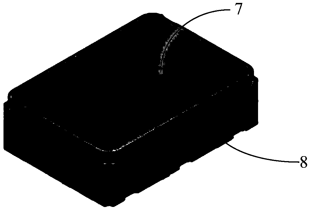
[0054] Embodiment 1: The insulating base 8 has a multi-layer structure, and the multi-layer structure of the insulating base 8 includes a bottom surface integrated with a plurality of discharge electrodes, at least one cavity layer on the bottom surface, and a solder layer on the top of the cavity layer . For example Figure 7 As shown in the example, the multilayer structure of the insulating base 8 includes a bottom surface 80 integrated with a plurality of discharge electrodes, and three cavity layers (for example, a cavity layer 83, a cavity layer 84 and a cavity layer 85) on the bottom surface 80. , wherein the upper surface of the uppermost cavity layer 85 has a metallization layer), and the solder layer 86 on the upper part of the three cavity layers (for example, cavity layer 83, cavity layer 84 and cavity layer 85), At least one cavity layer has at least one vertical and / or lateral conductive strip (for example, semi-cylindrical, for example, Figure 7 As shown, the...
Embodiment 2
[0055] Embodiment 2: The insulating base 8 has a multi-layer structure, and the multi-layer structure of the insulating base 8 includes a bottom surface integrated with a plurality of discharge electrodes, at least one cavity layer on the bottom surface, a solder layer on the top of the cavity layer, and the metal ring on top of the solder layer. For example Figure 9 As shown in the example, the multilayer structure of the insulating base 8 includes a bottom surface 80 integrated with a plurality of discharge electrodes, and three cavity layers (for example, a cavity layer 83, a cavity layer 84 and a cavity layer 87) on the bottom surface 80. ), the upper surface of the uppermost cavity layer 87 has a solder layer 89), and the metal ring 88 on the upper part of the solder layer 89, at least one cavity layer has at least one vertical and / or lateral conductive strip (in the form of a semi-cylindrical For example, for example, Figure 9 As shown, the cavity layer 84 has a plur...
Embodiment 3
[0056] Embodiment 3: The insulating base 8 has an integral structure (not shown in the figure), and the insulating base 8 includes an integral bottom surface, a cavity, and a solder layer, wherein the bottom surface is integrated with a plurality of discharge electrodes, and the cavity The upper part is a solder layer, and the cavity has at least one vertical and / or horizontal conductive strip (for example, a semi-cylindrical shape). The conductive upper cover 7 is sealed on the solder layer to form a closed cavity, and the formed closed cavity is used Filled with inert gas.
PUM
 Abstract
Description
Claims
Application Information
 - R&D
- Intellectual Property
- Life Sciences
- Materials
- Tech Scout
- Unparalleled Data Quality
- Higher Quality Content
- 60% Fewer Hallucinations
Browse by: Latest US Patents, China's latest patents, Technical Efficacy Thesaurus, Application Domain, Technology Topic, Popular Technical Reports.
© 2025 PatSnap. All rights reserved.Legal|Privacy policy|Modern Slavery Act Transparency Statement|Sitemap|About US| Contact US: help@patsnap.com


