Method for manufacturing floating gate MOS transistor

A technology of MOS transistors and manufacturing methods, which is applied in the field of manufacturing floating gate transistors, can solve problems such as cumbersome preparation methods and long production cycles, and achieve the effects of simplifying the process flow, improving production efficiency, and shortening delivery time

Inactive Publication Date: 2013-12-11
SHANGHAI HUALI MICROELECTRONICS CORP
View PDF4 Cites 5 Cited by
  • Summary
  • Abstract
  • Description
  • Claims
  • Application Information

AI Technical Summary

Problems solved by technology

This shows that the preparation method of the prior art is more loaded down with trivial details, and the production cycle is longer

Method used


Image

  • Method for manufacturing floating gate MOS transistor
  • Method for manufacturing floating gate MOS transistor
  • Method for manufacturing floating gate MOS transistor

Examples


Embodiment Construction

[0032] The specific embodiment of the present invention will be further described below in conjunction with accompanying drawing:

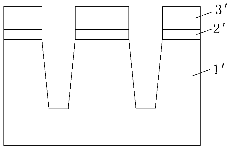
[0033] The invention provides a method for preparing a floating gate MOS transistor, which can be applied to the technical platform of Flash (memory) and eFlash, and includes the following steps:

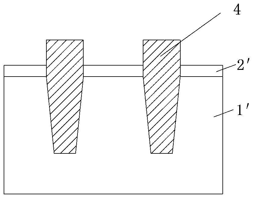
[0034] Step 1. Provide a silicon substrate 1. After depositing a layer of dielectric layer 2 on the upper surface of the silicon substrate, a polysilicon layer 6 and a nitride layer 7 are sequentially deposited on the surface of the dielectric layer 2 from bottom to top. Preferably, the thickness of the deposited polysilicon layer 6 is 600-700 angstroms (such as 600 angstroms, 630 angstroms, 650 angstroms, 680 angstroms, 700 angstroms), and the nitride layer 7 is silicon nitride, such as Figure 6 shown.

[0035] Step 2, coating a layer of photoresist to cover the upper surface of the nitride layer 7, performing an exposure and development process to f...


PUM

PropertyMeasurementUnit
thicknessaaaaaaaaaa

Abstract

The invention discloses a method for manufacturing a floating gate MOS transistor. The method includes the following steps that a medium layer, a polycrystalline silicon layer and a nitride layer are sequentially deposited on the surface of a silicon substrate; the nitride layer, the polycrystalline silicon layer and the medium layer are sequentially etched into the silicon substrate, and STI trenches are formed; an oxidation layer is deposited, the STI trenches are filled with the oxidation layer, and the oxidation layer covers the surface of the remaining nitride layer; a flattening technology is performed on the silicon oxide layer, and the remaining silicon oxide layer located on the surface of the remaining nitride layer is removed; after part of the silicon oxide layer located in the STI trenches is etched, the remaining nitride layer is removed. According to the method, the deposition steps are firstly performed, then the scheme of synchronous etching is adopted, and FG and STI technologies are finished at the same time. In comparison with a traditional technology, the technological processes are simplified, production efficiency is further improved, production time of finished products is shortened, and economic benefits are improved.

Description

technical field [0001] This field relates to the field of semiconductor manufacturing, in particular to a method for manufacturing a floating gate transistor. Background technique [0002] With the development of integrated circuit technology, the traditional silicon integrated circuit based on the function of a single transistor has many difficult and urgent problems to be solved, and the floating gate MOS transistor (Floating Gate MOS), as a new type of highly integrated unit transistor , which provides an effective way to solve the problems caused by the increase in the number of transistors and interconnection lines in integrated circuits. [0003] In the floating gate MOS transistor, since the FG (floating gate) is located above the STI (shallow trench isolation structure) and is completely opposite to the position of the STI, the traditional process for forming the FG is to first perform the STI Etch (shallow trench isolation structure). trench isolation structure etc...

Claims


Application Information

Patent Timeline
Patent Type & Authority Applications(China)
IPC IPC(8): H01L21/336H01L21/28H01L21/762
Inventor 秦伟高慧慧杨渝书黄海辉
Owner SHANGHAI HUALI MICROELECTRONICS CORP
Why Eureka
Try Eureka