

Simulation method of LDMOS (laterally diffused metal oxide semiconductor) array
A simulation method and array technology, applied in special data processing applications, instruments, electrical digital data processing, etc., can solve uneven current distribution, difficult LDMOS array simulation, and inability to accurately calculate the total equivalent of the drain drift region of the LDMOS array Width and other issues to achieve the effect of improving design efficiency, flexibility and precision
- Summary
- Abstract
- Description
- Claims
- Application Information
AI Technical Summary
Problems solved by technology
Method used
Image

Examples
Embodiment 1
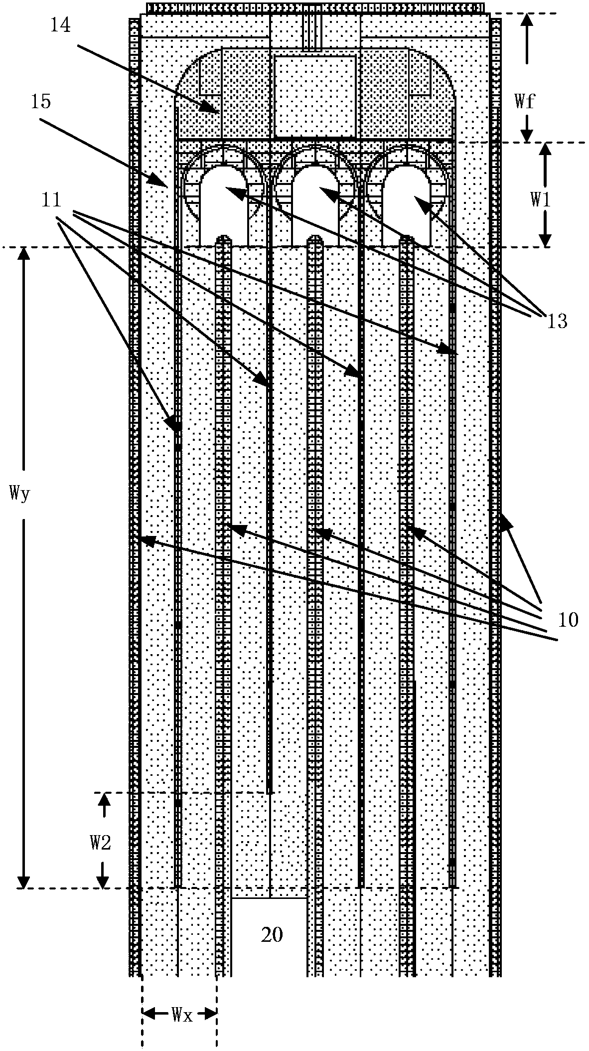
[0041] The structure of an LDMOS array is as figure 1 , figure 2 As shown, this kind of LDMOS array is formed by a plurality of individual LDMOSs connected in parallel, and this kind of LDMOS array includes a drain drift region 15, a drain metal layer 14, N arched gates 13, and N+1 rows of vertical drain contact holes. 11. N+2 rows of longitudinal source contact holes 10, a source pad (PAD) 20, where N is an integer greater than or equal to 2;
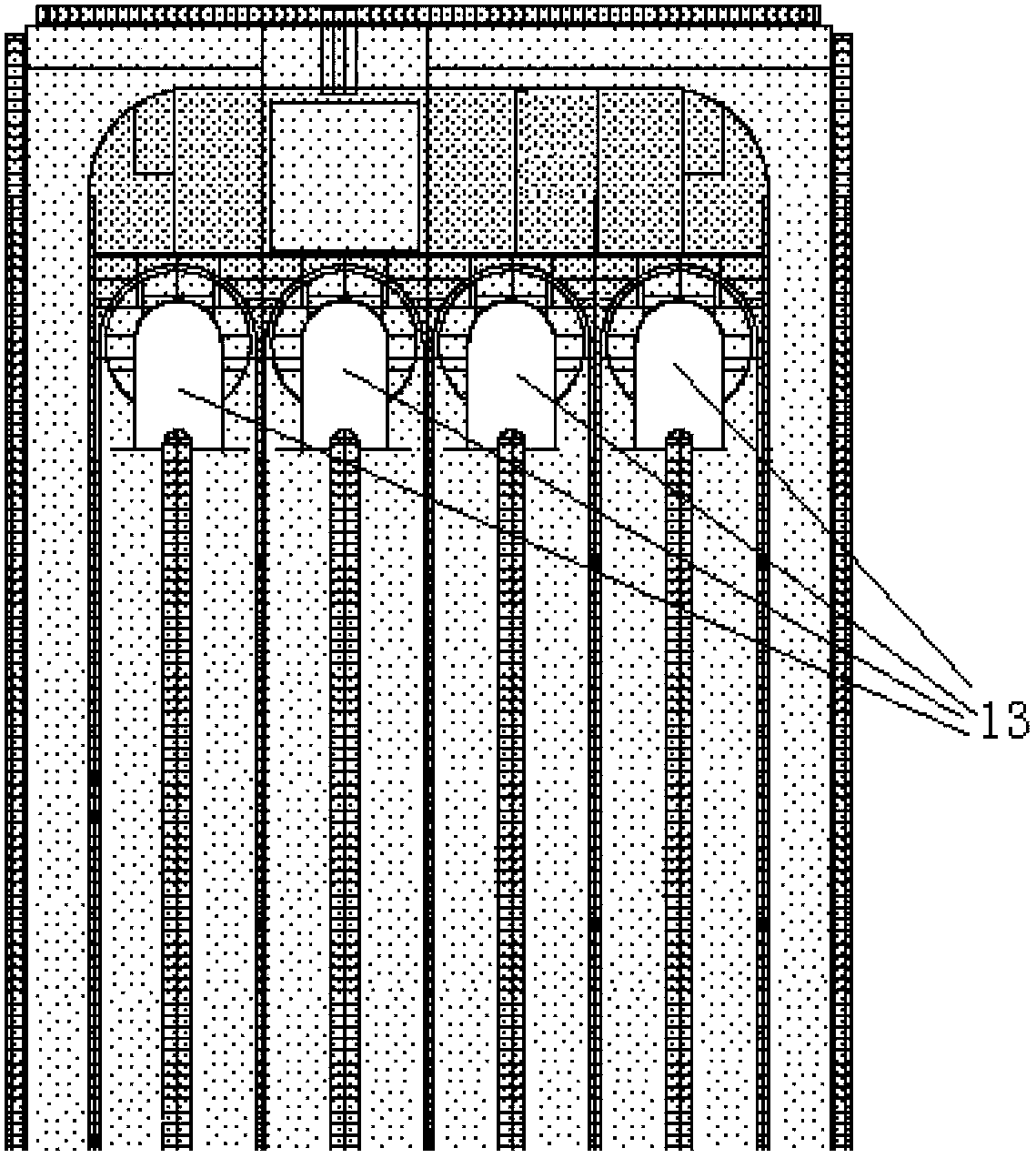
[0042] An arched door 13 is respectively arranged between the tops of two adjacent rows of vertical drain contact holes 11. The bottom ends of each arched door 13 are flush, and the middle is hollowed out and a field oxide layer grows, the purpose is to reduce the parasitic resistance of the drain end. ;
[0043] N+1 rows of vertical drain contact holes 11 are longitudinally distributed in the drain drift region 15 and equally spaced;
[0044] N+1 rows of vertical drain terminal contact holes are longitudinally distributed in the dra...
Embodiment 2
[0057] Using the macro model, simulate the saturation current value of the LDMOS array of multiple groups of different Wy and / or N under the same bias voltage, through the actual detection of the corresponding saturation current value of the LDMOS array under the same bias voltage Fitting, correcting the correction parameter Wf, and finally making the macro model obtain better accuracy under various Wy and N conditions, such as Figure 4 .
Embodiment 3
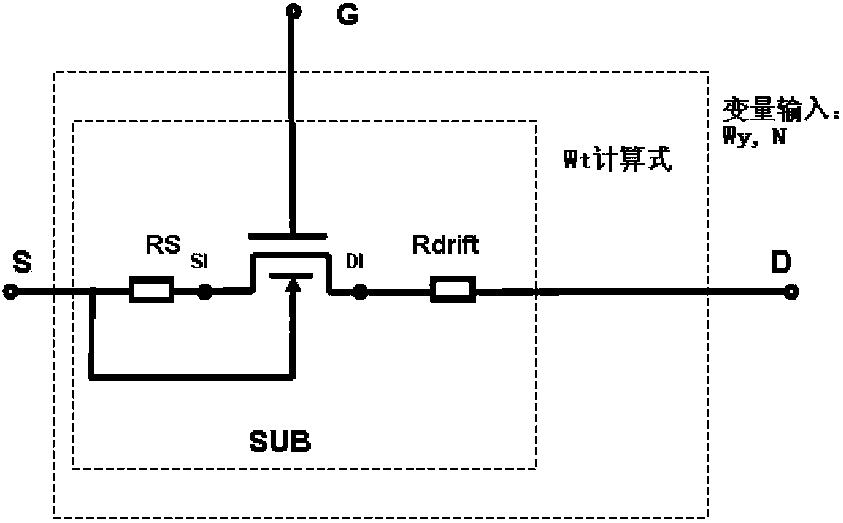
[0059] The LDMOS subcircuit model can be as image 3 As shown, it consists of a basic MOS transistor, a source terminal parasitic resistance RS, and a drain terminal parasitic resistance Rdrift. The source terminal parasitic resistance RS is connected in series between the source terminal S of the LDMOS sub-circuit and the source terminal SI of the basic MOS tube. The parasitic resistance Rdrift of the drain terminal is connected in series between the drain terminal D of the LDMOS sub-circuit and the drain terminal DI of the basic MOS transistor, and the source terminal S of the LDMOS sub-circuit is short-circuited with the substrate SUB of the basic MOS transistor;
[0060] The basic MOS transistor may adopt a BSIM3 model commonly used in the industry.
[0061] Preferably, the LDMOS sub-circuit model and the macro model are established with SPICE language.
[0062] The simulation method of a kind of LDMOS array of the present invention, at first according to the characterist...
PUM
 Abstract
Description
Claims
Application Information