Check patentability & draft patents in minutes with Patsnap Eureka AI!

Target material processing method

A processing method and target technology, applied in metal material coating process, ion implantation plating, coating and other directions, can solve problems such as affecting product quality, easy to produce abnormal discharge, etc., and achieve the effect of uniform distribution and large roughness

Active Publication Date: 2014-01-01
KONFOONG MATERIALS INTERNATIONAL CO LTD
View PDF8 Cites 19 Cited by
  • Summary
  • Abstract
  • Description
  • Claims
  • Application Information

AI Technical Summary

Problems solved by technology

[0005] However, after the surface of the existing target material is rough-dried by sandblasting, there are limitations in the adsorption capacity of the deposits, and in the case of complicated semiconductor manufacturing processes, problems such as abnormal discharge are still prone to occur, which seriously affects the quality of the product. quality

Method used


Image

  • Target material processing method
  • Target material processing method
  • Target material processing method

Examples


Embodiment Construction

[0025] In order to make the above objects, features and advantages of the present invention more comprehensible, specific implementations of the present invention will be described in detail below in conjunction with the accompanying drawings.

[0026] In the following description, numerous specific details are set forth in order to provide a thorough understanding of the present invention. However, the present invention can be implemented in many other ways different from those described here, and those skilled in the art can make similar extensions without violating the connotation of the present invention, so the present invention is not limited by the specific implementations disclosed below.

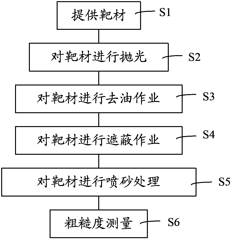
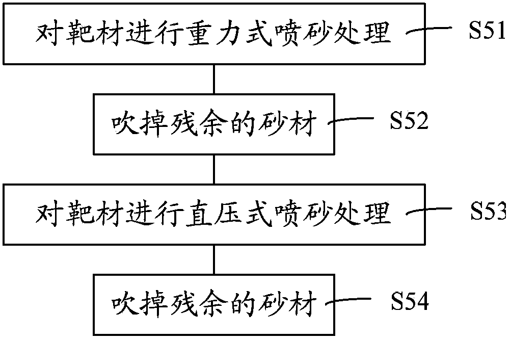
[0027] The flow chart of the embodiment of the target processing method of the present invention is as follows figure 1 with figure 2 As shown, it specifically includes the following steps:

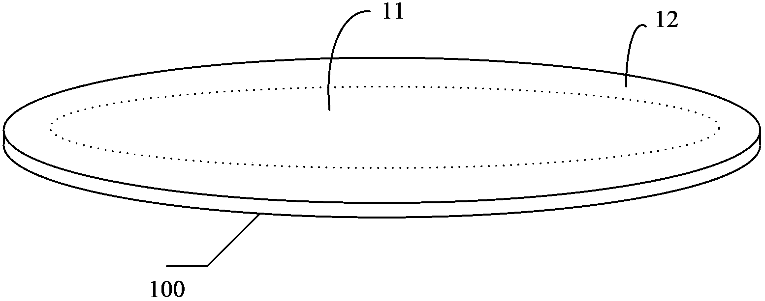
[0028] Step S1: providing a target.

[0029] The target material 100 provided can be as...


PUM

PropertyMeasurementUnit
Thicknessaaaaaaaaaa

Abstract

A target material processing method comprises the following steps: providing a target material, wherein a sputtering surface of the target material comprises a sandblasted area and a non-sandblasted area; and carrying out sandblast treatment of the area for sandblast of the target material, wherein the sandblast treatment comprises a process of gravity type sandblast treatment and a process of direct pressure type sandblast treatment. A surface having a small roughness is formed on the surface of the target material through the gravity type sandblast treatment and the roughness is increased through the direct pressure type sandblast treatment, so the roughness is uniformly distributed, and a large roughness can be easily realized.

Description

technical field [0001] The invention relates to the field of semiconductor manufacturing, in particular to a method for processing a target. Background technique [0002] In the process of manufacturing semiconductor devices, sputtering is a very important thin film formation process. The basic mechanism is that the target is bombarded by appropriate high-energy particles (electrons, ions, neutral particles), and the atoms on the surface may obtain enough energy to escape from the surface by colliding with high-energy particles, and then under the electric field force or magnetic force under the action of migrating to the silicon wafer. The physical process of sputtering to prepare thin films includes the following six basic steps: 1. Ions are generated in the plasma of the high vacuum chamber and accelerated to the target material with negative potential; 2. During the acceleration process, the ions gain momentum and bombard the target ;3. Ions knock out (sputtering) atom...

Claims


Application Information

Patent Timeline
IPC IPC(8): B24C1/06B24C5/02B24C11/00C23C14/34
Inventor 姚力军相原俊夫大岩一彦潘杰王学泽高建
Owner KONFOONG MATERIALS INTERNATIONAL CO LTD
Features
  • R&D
  • Intellectual Property
  • Life Sciences
  • Materials
  • Tech Scout
  • Unparalleled Data Quality
  • Higher Quality Content
  • 60% Fewer Hallucinations
Learn More