Silicon oxynitride insulation structure and manufacturing method thereof

A production method, a technology of silicon oxynitride, applied in semiconductor/solid-state device manufacturing, electrical components, circuits, etc., can solve the problems that the carrier tunneling effect cannot be improved, and achieve the effect of preventing tunneling effect and boron diffusion

Inactive Publication Date: 2014-01-01
SHANGHAI HUALI MICROELECTRONICS CORP
View PDF2 Cites 5 Cited by
  • Summary
  • Abstract
  • Description
  • Claims
  • Application Information

AI Technical Summary

Problems solved by technology

A silicon dioxide layer 22 is formed on the silicon substrate 20, and nitrogen ions are generated by using radio frequency voltage or current, and a silicon oxynitride layer 23 is formed on the surface of the silicon dioxide layer 22, which can effectively increase the nitrogen content on the surface of the silicon dioxide layer 22 , but cannot improve the tunneling effect of carriers between the silicon dioxide layer 22 and the silicon substrate 20

Method used


Image

  • Silicon oxynitride insulation structure and manufacturing method thereof
  • Silicon oxynitride insulation structure and manufacturing method thereof
  • Silicon oxynitride insulation structure and manufacturing method thereof

Examples


Embodiment Construction

[0034] The problem to be solved by the present invention is to provide a silicon oxynitride insulating structure and a manufacturing method thereof, which can prevent the tunneling effect of carriers while preventing boron diffusion.

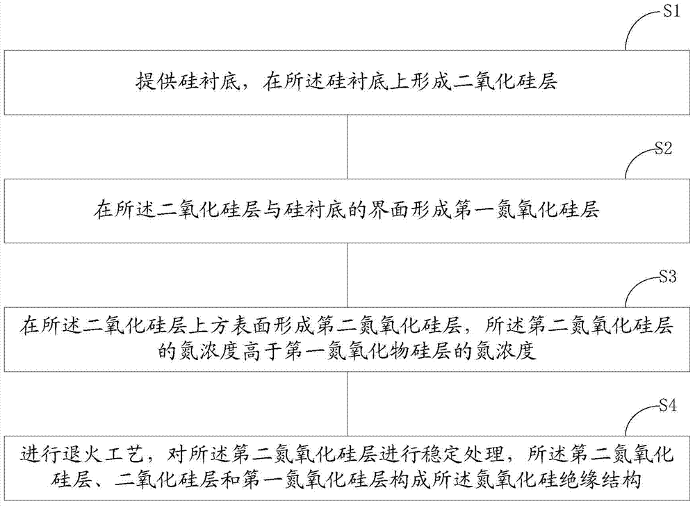
[0035] In order to solve the above problems, the present invention provides a method for fabricating a silicon oxynitride insulating structure, please refer to image 3 A schematic flow chart of a method for manufacturing a silicon oxynitride insulating structure according to an embodiment of the present invention is shown, and the method includes:

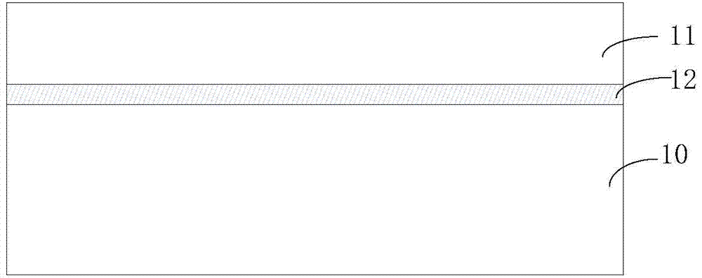
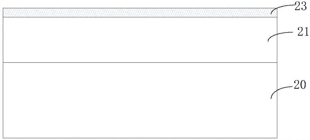
[0036] Step S1, providing a silicon substrate, and forming a silicon dioxide layer on the silicon substrate;

[0037] Step S2, forming a first silicon oxynitride layer at the interface between the silicon dioxide layer and the silicon substrate;

[0038] Step S3, forming a second silicon oxynitride layer on the surface above the silicon dioxide layer, the nitrogen concentration of the second silico...


PUM


Abstract

The invention provides a silicon oxynitride insulation structure and a manufacturing method of the silicon oxynitride insulation structure. The manufacturing method includes the steps that a silicon substrate is provided, and a silicon dioxide layer is formed on the silicon substrate; a first silicon oxynitride layer is formed on the interface between the silicon dioxide layer and the silicon substrate; a second ilicon oxynitride layer is formed on the upper surface of the silicon dioxide layer, and the nitrogen concentration of the second ilicon oxynitride layer is larger than that of the first silicon oxynitride layer; stabilizing processing is carried out on the second ilicon oxynitride layer by an annealing process, and silicon oxynitride insulation structure is composed of the second ilicon oxynitride layer, the silicon dioxide layer and the first silicon oxynitride layer and can prevent the tunnelling effect of carriers while preventing boron diffusion.

Description

technical field [0001] The invention relates to the technical field of semiconductors, in particular to a silicon oxynitride insulating structure and a manufacturing method thereof. Background technique [0002] At present, silicon dioxide is the main material of the gate insulating layer. As the integration level of integrated circuits continues to increase and the critical dimensions continue to decrease, the thickness of the silicon dioxide layer becomes smaller and smaller. Since the silicon dioxide layer of the gate insulating layer becomes thinner, the boron dopant of the gate electrode easily penetrates the thin silicon dioxide layer, and the tunneling effect of carriers is prone to occur. It is no longer feasible to use the traditional pure silicon dioxide layer as the gate insulating layer. In order to overcome the above problems, the prior art generally adopts nitrogen doping in the silicon dioxide layer to reduce the diffusion of dopants and increase its dielectr...

Claims


Application Information

Patent Timeline
Patent Type & Authority Applications(China)
IPC IPC(8): H01L21/285H01L29/51
CPCH01L21/28158H01L29/513H01L29/518
Inventor 江润峰
Owner SHANGHAI HUALI MICROELECTRONICS CORP
Why Eureka
Try Eureka