Low electric field source erasable non-volatile memory and methods for producing same

a non-volatile memory, low electric field technology, applied in the direction of semiconductor devices, electrical apparatus, transistors, etc., can solve the problems of large operating current required during the erasing operation, leakage current from the source to the substrate, and difficulties in the integration of the whole circuit, so as to avoid a high electric field

Active Publication Date: 2017-05-02
XINNOVA TECH
View PDF3 Cites 1 Cited by
  • Summary
  • Abstract
  • Description
  • Claims
  • Application Information

AI Technical Summary

Benefits of technology

[0007]An objective of the present invention is to overcome the drawbacks of the conventional techniques by providing a low electric field source erasable non-volatile memory unit which can use the erasing operation voltage and the tip voltage effect of the floating gate to avoid electrons from tunneling to the source lightly-doped region while avoiding a high electric field resulting from overlapping of the source heavily-doped region and the floating gate and the resultant GIDL.
[0055]In the present invention, under the source erasing operation, since the polycrystalline silicon of the floating gate pointed to the source diffusion region has a tip voltage effect, overlapping of the tip electric field of the floating gate required by the tunneling with the heavily-doped region of the source diffusion region is not so influential. The effects of the low electric field source erasable non-volatile memory unit of the present invention are that since the floating gate only overlaps with the lightly-doped region of the source diffusion region and is misaligned from the heavily-doped region in a horizontal or vertical direction, intensities of the horizontal and vertical electric fields between the source and the p-type silicon substrate can effectively be reduced. Thus, the leakage current from the source diffusion region to the p-type silicon substrate resulting from the GIDL effect can effectively be reduced to reduce the current supply demand of the power source, permitting easy achievement of integration of the whole circuit.

Problems solved by technology

Firstly, an over erasure effect exists.
When the memory unit undergoes the erasing operation, excessive electrons could be removed from the floating gate, resulting in a negative threshold voltage of an equivalent transistor component in the memory unit; namely, the memory unit is normally in a conductive state that leads to unnecessary leakage current.
Secondly, a larger operating current is required during the erasing operation.
When the memory undergoes the erasing operation, the source voltage is much larger than the voltage of the floating gate and, thus, results in a gate-induced drain leakage (GIDL) effect, leading to leakage current from the source to the substrate.
As a result, an external power source more powerful in providing current is required in the operation, leading to difficulties in integration of the whole circuit.
However, as the processes are more and more advanced and the size becomes smaller and smaller, the lightly-doped drain is apt to cause a punch-through effect.
Due to the structural limitation, the memory units sharing the deep N-well must simultaneously undergo the erasing operation, which sacrifices the operational flexibility of the circuit.
However, as the processes are more and more advanced and the size becomes smaller and smaller, the lightly-doped drain is apt to cause a punch-through effect.
However, during conduction of an equivalent transistor component of the non-volatile memory unit, the magnitude of the conduction current is decided by a thicker gate dielectric layer formed by the wedge structure, such that the change in the conduction current is larger and, thus, adversely affects the yield of the memories.
Furthermore, the thicker tunnel dielectric layer of the stepped floating gate is liable to cause a short circuit between the drain and the source, resulting in great limitation to further miniaturization of the structure.

Method used


Image

  • Low electric field source erasable non-volatile memory and methods for producing same
  • Low electric field source erasable non-volatile memory and methods for producing same
  • Low electric field source erasable non-volatile memory and methods for producing same

Examples


first embodiment

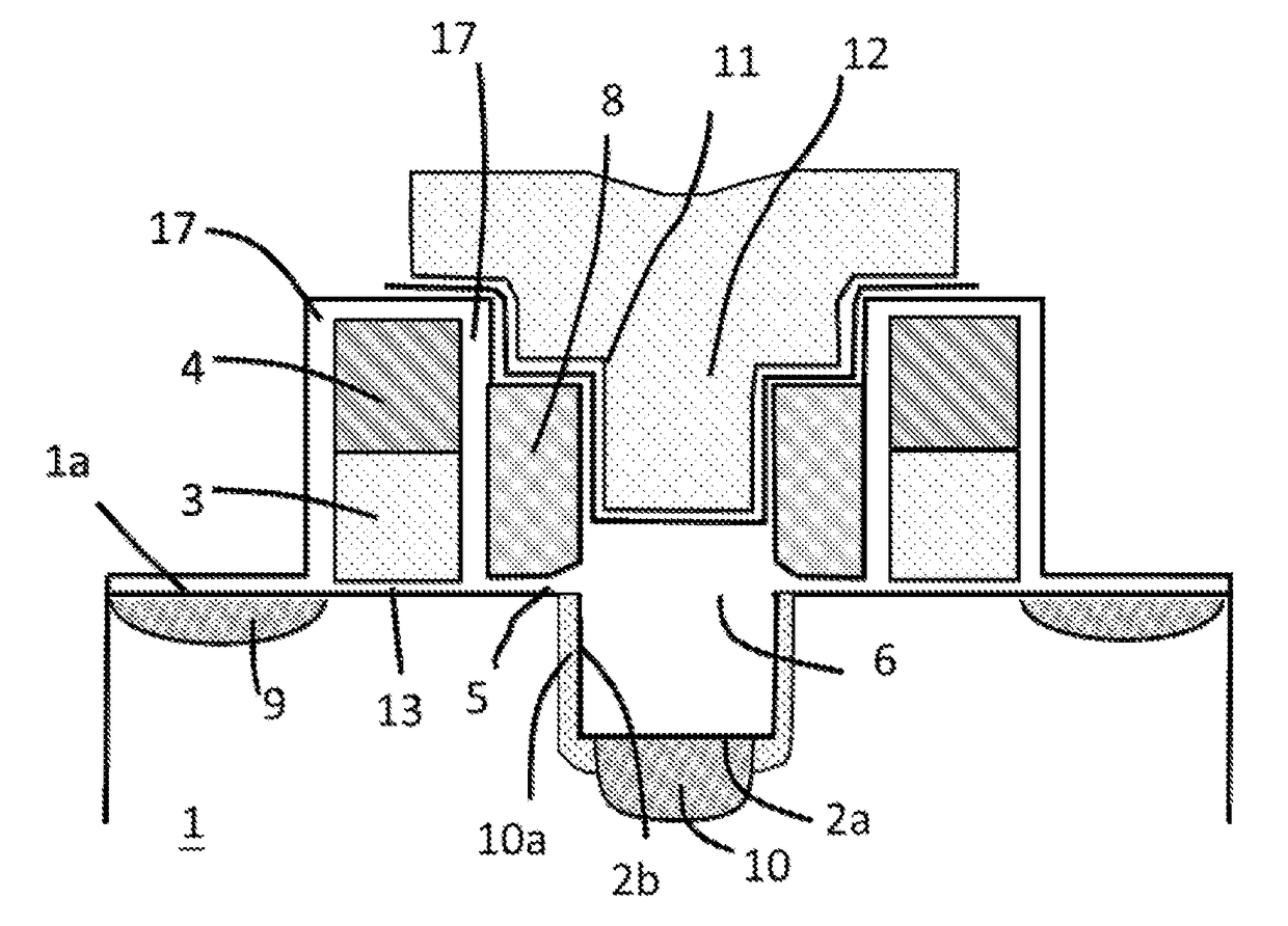
[0101]FIG. 3 is a diagrammatic cross sectional view of a low electric field source erasable non-volatile memory unit of a first embodiment according to the present invention.

[0102]Please refer to FIG. 3 showing two low electric field source erasable non-volatile memory units symmetric to each other. Description of the low electric field source erasable non-volatile memory unit at the left part of the figure will be set forth. The low electric field source erasable non-volatile memory unit includes a substrate that is generally a p-type silicon substrate 1. The p-type silicon substrate 1 includes an upper surface 1a. In the p-type silicon substrate 1, a drain diffusion region 9 is formed by an n-type doped layer, and a source diffusion region 10 is formed by another n-type doped layer. The source diffusion region 10 includes a lightly-doped region 10a that is a lightly-doped n-type region (source lightly n-doped diffusion). The drain diffusion region 9 is not contiguous to the source...

second embodiment

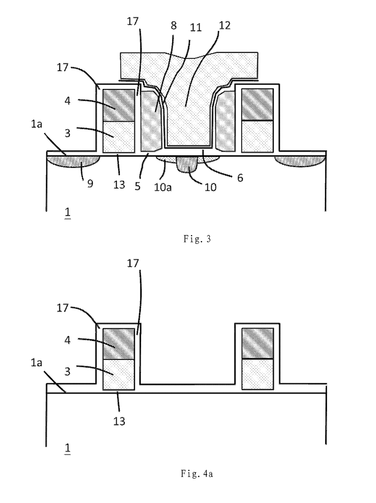
[0124]FIG. 5 is a diagrammatic cross sectional view of a low electric field source erasable non-volatile memory unit of a second embodiment according to the present invention.

[0125]An example of the method for producing the low electric field source erasable non-volatile memory unit of the second embodiment will now be set forth in connection with FIGS. 6a-6i.

[0126]The formation step shown in FIG. 6a is the same as that shown in FIG. 4a. Please refer to the corresponding description in connection with FIG. 4a.

[0127]The formation step shown in FIG. 6b is the same as that shown in FIG. 4b. Please refer to the corresponding description in connection with FIG. 4b.

[0128]As shown in FIG. 6c, a flat polycrystalline silicon layer 7 is formed on the face of the structure of FIG. 6b by chemical vapor deposition (CVD) and etch back or chemical-mechanical polishing (CMP). The upper face of the polycrystalline silicon layer 7 above the first insulating layer 4 and the floating gate 3 has an e...


PUM


Abstract

A low electric field source erasable non-volatile memory unit includes a substrate having a source diffusion region and a drain diffusion region. The source diffusion region includes a heavily-doped region and a lightly-doped region extending. A first dielectric layer and a tunnel dielectric layer are formed on the substrate. The tunnel dielectric layer includes a lower face contiguous to or partially overlapped with the lightly-doped region of the source diffusion region. A select gate and a floating gate are respectively formed on the first dielectric layer and the tunnel dielectric layer. The floating gate includes a source side edge contiguous to or partially overlapped with the lightly-doped region and misaligned from the heavily-doped region by a distance. A second dielectric layer and a control gate are formed on the floating gate. The control gate and the floating gate are insulating to each other by the second dielectric layer.

Description

BACKGROUND OF THE INVENTION[0001]The present invention relates to a structure of an integrated circuit component and its producing methods and, more particularly, to a low electric field source erasable non-volatile memory and methods for producing the low electric field source erasable non-volatile memory.[0002]Non-volatile memories have advantages of small volumes, light weights, low power consumption, and prevention of loss of data resulting from power interruption and are, thus, suitable for applications in hand-held electronic devices. Following the popularization of hand-held electronic devices, non-volatile memories have widely been used as multimedia storage devices or used for maintaining normal operation of electronic systems. The need of non-volatile memories increases every year, and the costs and prices decrease, which is a positive cycle for non-volatile memories. Thus, non-volatile memories have become one of the most important products in the semiconductor industry.[...

Claims


Application Information

Patent Timeline
Patent Type & Authority Patents(United States)
IPC IPC(8): H01L21/28H01L29/66H01L29/788H01L27/11521H01L29/423H01L21/308H01L21/265
CPCH01L21/28273H01L27/11521H01L29/42328H01L29/66825H01L29/7883H01L29/7889H01L21/2652H01L21/3086H10B41/35H01L29/40114H10B41/30
Inventor FAN, DER-TSYRCHEN, CHIH-MINGLU, JUNG-CHANG
Owner XINNOVA TECH
Why Eureka
Try Eureka