Array substrate, manufacturing method thereof and display device

A technology for array substrates and manufacturing methods, applied in the fields of array substrates and their manufacturing methods, and display devices, can solve problems such as poor channels, affecting product quality, and failure to improve mask output, so as to reduce manufacturing processes, improve product quality, and Avoid the effect of TFT channel bad

Active Publication Date: 2014-01-01
BEIJING BOE OPTOELECTRONCIS TECH CO LTD
View PDF4 Cites 15 Cited by
  • Summary
  • Abstract
  • Description
  • Claims
  • Application Information

AI Technical Summary

Problems solved by technology

[0005] It can be seen that for the current TFT-LCD array substrate manufacturing process, when preparing products with high PPI and containing GOA, 7mask is often used in the preparation process for factors such as dense wiring, so it is often not available due to the large number of masks. Improvement; moreover, the formation of channels in the existing TFT-LCD array substrates is formed by etching, often due to reasons such as processes and equipment in the etching process, channel defects are often caused, and such defects often occur frequently in production lines, affect product quality

Method used


Image

  • Array substrate, manufacturing method thereof and display device
  • Array substrate, manufacturing method thereof and display device
  • Array substrate, manufacturing method thereof and display device

Examples


Embodiment Construction

[0088] The principles and features of the present invention are described below in conjunction with the accompanying drawings, and the examples given are only used to explain the present invention, and are not intended to limit the scope of the present invention.

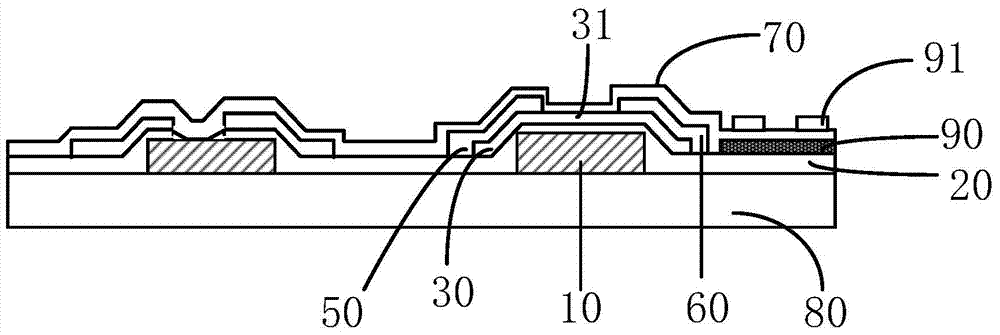
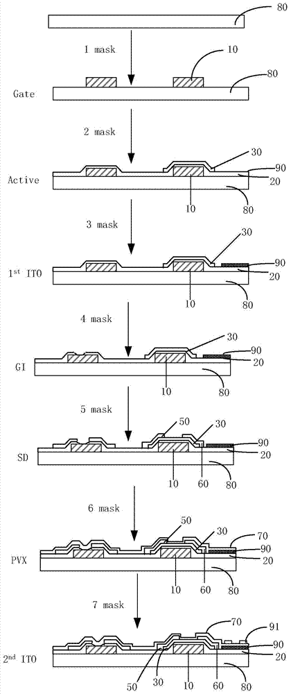
[0089] It should be noted that the "upper" in "X is arranged on Y" mentioned in the present invention includes the meaning that X is in contact with Y and that X is located above Y. In the present invention, as shown in the accompanying drawings, the The base substrate is defined as being arranged at the bottom; the patterning process referred to in the present invention includes processes such as photoresist coating, masking, exposure, development, etching, and photoresist stripping. as an example.

[0090] Preferred embodiments of the TFT-LCD array substrate provided by the present invention are described below.

[0091] The TFT-LCD array substrate of this embodiment mainly includes gate lines, data lines, TFTs a...


PUM


Abstract

The invention provides an array substrate, a manufacturing method thereof and a display device. The manufacturing method comprises the steps that a grid metal film is deposited on a substrate body, and a first graph comprising a grid is formed through a primary composition technology; a grid insulating film, a first transparent conductive film, a source drain metal film and a doped a-si film are sequentially deposited, and a second graph comprising a pixel electrode, a source, a drain and a doped semiconductor layer is formed through a secondary composition technology; the a-si film is deposited, and a third graph comprising a TFT channel, a semiconductor layer and a grid insulating layer via hole is formed through a third composition technology; a passivation layer film is deposited and a fourth graph comprising a passivation layer via hole is formed through a fourth composition technology, wherein the passivation layer film via hole corresponds to the grid insulating layer via hole in position; a second transparent conductive layer is deposited and a fifth graph comprising an electric connecting part is formed through a fifth composition technology. By means of the manufacturing method, manufacturing processes can be reduced and the product quality can be improved.

Description

technical field [0001] The present invention relates to the field of display technology, in particular to an array substrate, a manufacturing method thereof, and a display device. Background technique [0002] A Thin Film Transistor Liquid Crystal Display (TFT-LCD for short) is a main flat panel display device. The existing array substrate (Array Substrate) includes: gate lines, data lines, thin film transistors (Thin Film Transistor, TFT for short) and pixel electrodes. The gate lines are arranged laterally on the base substrate, the data lines are vertically arranged on the base substrate, and TFTs are arranged at intersections of the gate lines and the data lines. TFT is an active switching element. [0003] like figure 1 As shown, the existing array substrate includes: a gate 10 , a gate insulating layer 20 , an active layer 30 , a source electrode 50 , a drain electrode 60 , and a passivation layer 70 . The above structures are all disposed on the base substrate 80 ...

Claims


Application Information

Patent Timeline
Patent Type & Authority Applications(China)
IPC IPC(8): H01L27/12H01L21/77G02F1/1362G02F1/1368
CPCH01L27/124H01L27/1288H01L27/1218H01L27/1248H01L27/1262
Inventor 李田生谢振宇
Owner BEIJING BOE OPTOELECTRONCIS TECH CO LTD
Why Eureka
Try Eureka