Wafer-level packaging method of image sensor chips

An image sensor and wafer-level packaging technology, applied in the semiconductor field, can solve problems such as fragile, dust pollution, and increase packaging costs, and achieve the effects of avoiding cutting, high reliability, and reducing production costs

Active Publication Date: 2014-01-01
格科微电子(浙江)有限公司
View PDF5 Cites 25 Cited by
  • Summary
  • Abstract
  • Description
  • Claims
  • Application Information

AI Technical Summary

Problems solved by technology

[0005] The wafer-level packaging method of the existing image sensor chip above has three disadvantages: 1. The above-mentioned packaging technology uses a whole piece of optical glass 105, and only the optical glass 105 provides strength, but because the overall brittleness of the glass is relatively large, the package The mechanical strength of the structure is low, it is easy to break, and the large piece of optical glass 105 is expensive, so the packaging cost is increased; 2. Since the cavity wall 103 is obtained by exposing and developing photosensitive materials, its raw material cost and process cost are relatively high, and the cavity wall 103 will be incompletely exposed during the manufacturing process, res

Method used


Image

  • Wafer-level packaging method of image sensor chips
  • Wafer-level packaging method of image sensor chips
  • Wafer-level packaging method of image sensor chips

Examples


Embodiment 2

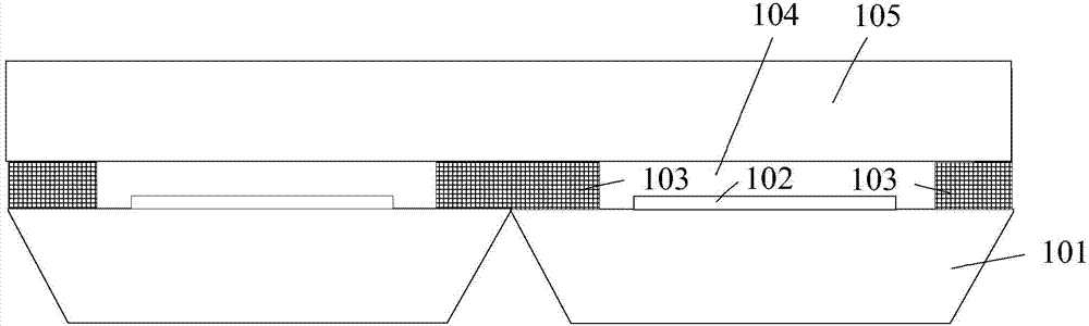
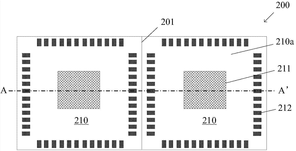
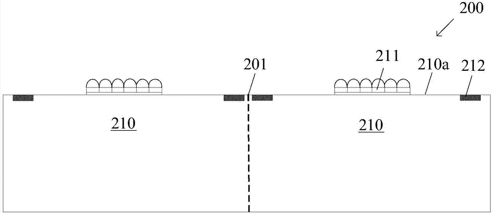
[0097] In the wafer-level packaging method of the image sensor chip provided in the second embodiment, a wafer, a mixed substrate and a carrier are also provided, and the wafer, the mixed substrate and the carrier can refer to the related content of the first embodiment, and, In this embodiment, similarly, the wafer, the hybrid substrate and the carrier are sequentially stacked and bonded together.

[0098] Same as the first embodiment, in this embodiment, the hybrid substrate and the carrier board are fixed together by spot glue. However, different from Embodiment 1, in this embodiment, after the redistribution line process and solder bump manufacturing process are performed on the wafer, and before the wafer and the mixed substrate are cut along the dicing line, the viscosity of the dispensing glue is reduced. In particular, the carrier is separated from the hybrid substrate, after which the wafer and hybrid substrate are diced.

[0099] Since this embodiment does not cut t...


PUM

PropertyMeasurementUnit
Thicknessaaaaaaaaaa

Abstract

A wafer-level packaging method of image sensor chips comprises the steps of providing wafers, mixed substrates and carrier plates. The wafers comprise a plurality of image sensor chips, and the mixed substrates comprise a supporting frame and a plurality of transparent substrate units. The supporting frame comprises a plurality of windows, the transparent substrate units cover the windows correspondingly, and the wafers, the mixed substrates and the carrier plates are fixed together in sequence in an overlapped mode. The back faces of the wafers are subjected to a line redistribution process and a welding flux protrusion manufacturing process, and the wafers and the mixed substrates are cut along cutting channels, so that the image sensor chips are separated to a plurality of image sensor chip modules which comprise separated mixed substrate units and image sensor chip units bonded with the mixed substrate units. By means of the method, the image sensor chips are maintained to be clean in the whole packaging process without being damaged, and the packaged image sensor chip modules have high reliability.

Description

technical field [0001] The invention relates to the technical field of semiconductors, in particular to a wafer-level packaging method for an image sensor chip. Background technique [0002] An image sensor is a device that converts one-dimensional or two-dimensional optical information (optical information) into electrical signals. Image sensors can be further divided into two different types: Complementary Metal Oxide Semiconductor (CMOS) image sensors and Charge Coupled Device (CCD) image sensors. Image sensor chips must be packaged to protect against corrosion, mechanical damage, dust particles, etc. The traditional image sensor chip packaging method is usually packaged by wire bonding (Wire Bonding), but with the rapid development of integrated circuits, longer leads make the product size unable to meet the ideal requirements. [0003] Wafer Level Package (WLP) is a packaging method in which after the front-end process of the wafer is completed, the back-end process i...

Claims


Application Information

Patent Timeline
IPC IPC(8): H01L27/146H01L23/04H01L21/683
CPCH01L2224/11
Inventor 赵立新李文强邓辉夏欢
Owner 格科微电子(浙江)有限公司
Why Eureka
Try Eureka