Thin film transistor, preparation method of thin film transistor, array substrate and display device

A technology of thin-film transistors and array substrates, which is applied in the display field, can solve problems affecting the characteristics of thin-film transistors, and achieve the effects of high density, less internal defects, and improved characteristics of thin-film transistors

Active Publication Date: 2014-01-01
BOE TECH GRP CO LTD
View PDF6 Cites 20 Cited by
  • Summary
  • Abstract
  • Description
  • Claims
  • Application Information

AI Technical Summary

Problems solved by technology

[0005] The object of the present invention is to provide a thin film transistor and its preparation method, an array substrate and a display device, so as to solve the defect state in the interface formed between the insulating layer of the thin film transistor and the metal oxide constituting the semiconductor layer in the prior art, thereby Problems Affecting the Characteristics of Thin Film Transistors

Method used


Image

  • Thin film transistor, preparation method of thin film transistor, array substrate and display device
  • Thin film transistor, preparation method of thin film transistor, array substrate and display device
  • Thin film transistor, preparation method of thin film transistor, array substrate and display device

Examples


Embodiment Construction

[0030] The implementation process of the embodiment of the present invention will be described in detail below in conjunction with the accompanying drawings. It should be noted that the same or similar reference numerals represent the same or similar elements or elements having the same or similar functions throughout. The embodiments described below by referring to the figures are exemplary only for explaining the present invention and should not be construed as limiting the present invention.

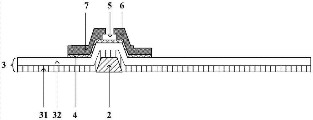
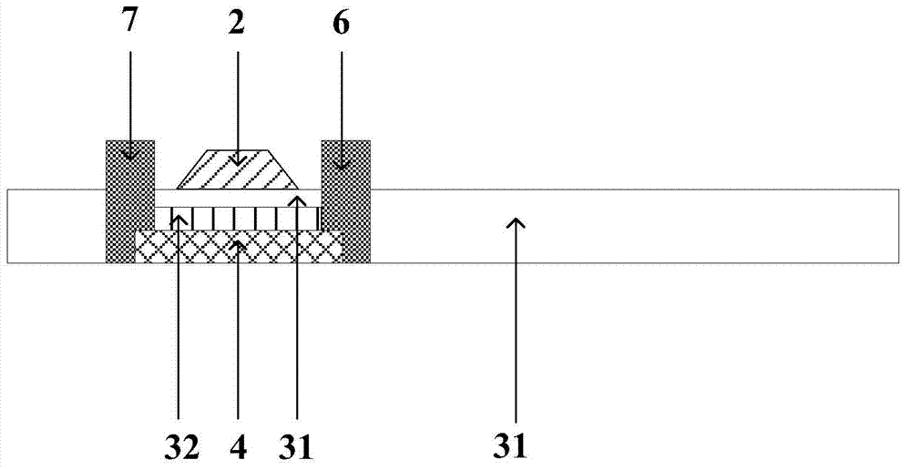
[0031] An embodiment of the present invention provides a thin film transistor to solve the problem in the prior art that defect states exist at the interface formed between the insulating layer of the thin film transistor and the metal oxide constituting the semiconductor layer, thereby affecting the characteristics of the thin film transistor. The thin film transistor provided by the embodiment of the present invention may have a bottom-gate structure or a top-gate structure.

[003...


PUM


Abstract

The invention discloses a thin film transistor. The thin film transistor comprises a grid electrode, a semiconductor layer and an insulating layer. The thin film transistor is characterized in that the insulating layer comprises a first insulating layer body composed of a first silicon oxide thin film and a second silicon oxide thin film, the second silicon oxide thin film directly makes contact with the semiconductor layer, and the compactness of the second silicon oxide thin film is larger than that of the first silicon oxide thin film. A good interface is formed between the second silicon oxide thin film and the semiconductor layer, defect states are reduced, and the features of the thin film transistor are improved. The embodiment of the invention further provides a preparation method of the thin film transistor, an array substrate and a display device.

Description

technical field [0001] The invention relates to the field of display technology, in particular to a thin film transistor, a preparation method thereof, an array substrate and a display device. Background technique [0002] Flat panel displays have replaced bulky cathode ray tube (Cathode Ray Tube, CRT) displays and are increasingly embedded in people's daily lives. Currently, commonly used flat panel displays include liquid crystal displays (Liquid Crystal Display, LCD) and organic light-emitting diode (Organic Light-Emitting Diode, OLED) displays. The above-mentioned flat-panel display has the characteristics of small size, low power consumption, and no radiation, and occupies a dominant position in the current flat-panel display market. [0003] With the rapid development of flat-panel displays, their size and resolution continue to increase, and at the same time, the frequency of the driving circuit is also continuously increased. The mobility of the existing amorphous s...

Claims


Application Information

Patent Timeline
Patent Type & Authority Applications(China)
IPC IPC(8): H01L29/786H01L29/423H01L29/51H01L21/336H01L21/285H01L27/12
CPCH01L21/285H01L29/513H01L29/66969H01L29/7869H01L27/1225H01L29/4908H01L29/42384H01L2029/42388H01L27/1262H01L29/78606
Inventor 刘翔
Owner BOE TECH GRP CO LTD
Why Eureka
Try Eureka