A kind of patterned substrate and LED chip for LED formal installation structure

A patterned substrate and LED chip technology, which is applied in the direction of electrical components, circuits, semiconductor devices, etc., can solve the problems of reducing the life of LED chips with internal quantum efficiency, high manufacturing costs of nanometer-level patterns, and limiting popularization and application. Effects of quantum efficiency, improvement of epitaxy quality, and excellent light extraction efficiency

Active Publication Date: 2017-01-25
SOUTH CHINA UNIV OF TECH
View PDF4 Cites 0 Cited by
  • Summary
  • Abstract
  • Description
  • Claims
  • Application Information

AI Technical Summary

Problems solved by technology

Studies have shown that as the pattern pitch decreases, voids are likely to appear at the interface between GaN and sapphire due to the lack of time for GaN growth to heal, and cause more dislocations in the epitaxial layer. Even if the light extraction efficiency is improved, the epitaxial layer position The increase of errors will reduce its internal quantum efficiency and LED chip life
In addition, the manufacturing cost of nanoscale patterns is high, and industrialization is relatively difficult, which greatly limits its popularization and application.

Method used


Image

  • A kind of patterned substrate and LED chip for LED formal installation structure
  • A kind of patterned substrate and LED chip for LED formal installation structure
  • A kind of patterned substrate and LED chip for LED formal installation structure

Examples


Embodiment 1

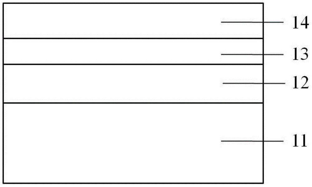
[0026] figure 1 It is a schematic diagram of the LED chip of this embodiment, which consists of a sapphire patterned substrate 11 , an N-type GaN layer 12 , an MQW quantum well layer 13 , and a P-type GaN layer 14 arranged in sequence.

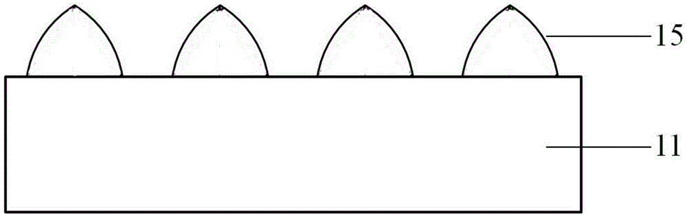
[0027] Such as figure 2 As shown, this embodiment is used for the sapphire patterned substrate 11 of the LED positive mounting structure, and the pattern of the substrate is composed of a plurality of dome-shaped patterns 15 of the same shape arranged on the surface of the substrate.

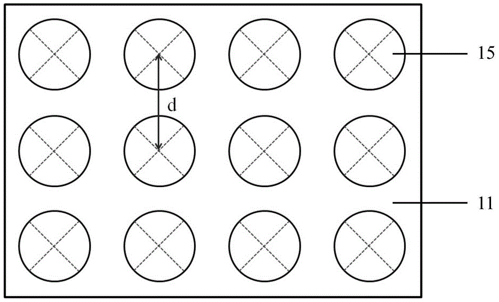
[0028] Such as Figure 3-4 As shown, the dome-shaped pattern is an axisymmetric cone, the bottom surface of the cone is a circle with a radius R of 1.2 μm, and the height h of the cone is 1.5 μm. Such as Figure 4 As shown, the cross-section of the vertebral body along the axis of symmetry is a triangular-like shape composed of two symmetrical arcs and a straight line. Point O in the figure is the center of the circle corresponding to the arc AB, and the cen...

Embodiment 2

[0032] In this embodiment, except the following features, all the other features are the same as in Embodiment 1:

[0033] The dome-shaped pattern is an axisymmetric cone, the base of the cone is a circle with a radius of 0.8 μm, and the height of the cone is 1.3 μm. The cross-section of the vertebral body along the axis of symmetry is a triangular-like shape composed of two symmetrical arcs and a straight line; the central angle corresponding to the arcs is 5°; the distance between adjacent vertebral bodies is 2.0 μm.

[0034] The test result of this embodiment is close to embodiment 1.

Embodiment 3

[0036] In this embodiment, except the following features, all the other features are the same as in Embodiment 1:

[0037] The dome-shaped pattern is an axisymmetric cone, the base of the cone is a circle with a radius of 1.2 μm, and the height of the cone is 1.6 μm. The cross-section of the vertebral bodies along the axis of symmetry is a triangular-like shape composed of two symmetrical arcs and a straight line; the central angle corresponding to the arcs is 15°; the distance between adjacent vertebral bodies is 4.0 μm.

[0038] The test result of this embodiment is close to embodiment 1.


PUM


Abstract

The invention discloses a patterned substrate used for an LED forwardly-installed structure. The pattern of the substrate is formed by a plurality of dome-type pattern bodies which are same in shape and are arranged on the surface of the substrate; the dome-type pattern bodies are axisymmetric cones, the bottom surface of each cone is a circle with the radius of 0.8-1.2 microns, and the height of each cone is 1.3-1.6 microns; the section, along the symmetric axis, of each cone is nearly a triangle which is formed by two symmetrical circular arcs and one linear segment; the corresponding central angle of each circular arc is 5-15 degrees. The invention further discloses the LED chip including the patterned substrate. Compared with the prior art, light-emitting efficiency is better, the external quantum efficiency of the LED chip is improved, screw dislocation is effectively restrained from being produced, the quality of epitaxial wafers is further improved, and therefore the internal quantum efficiency of an LED is enhanced.

Description

technical field [0001] The invention relates to an LED chip, in particular to a patterned substrate and an LED chip for an LED front mounting structure. Background technique [0002] As a new type of solid-state lighting source, LED is considered to be a green lighting source in the 21st century due to its low calorific value, low power consumption, fast response, long life, and small size. Facing the market demand for high-power lighting in the future, the luminous efficiency of LEDs needs to be improved. The light extraction efficiency of LED depends on internal quantum efficiency and external quantum efficiency. On the one hand, due to the large difference in the lattice constant and thermal expansion coefficient of GaN and sapphire substrates, the crystals of GaN thin films have a density of 10 9 -10 12 cm -2 traversing dislocations, which adversely affect the internal quantum efficiency of GaN-based LEDs. However, with the continuous optimization of GaN epitaxial g...

Claims


Application Information

Patent Timeline
Patent Type & Authority Patents(China)
IPC IPC(8): H01L33/48
CPCH01L33/20
Inventor 李国强王海燕周仕忠何攀贵乔田林志霆
Owner SOUTH CHINA UNIV OF TECH
Why Eureka
Try Eureka