Epitaxial structure, growth process and chip process of near-infrared light emitting diode
A technology of light-emitting diodes and epitaxial structures, applied in crystal growth, single crystal growth, electrical components, etc., can solve problems such as difficulty in meeting the high power requirements of near-infrared light-emitting diodes, low internal quantum efficiency of near-infrared diodes, and difficult breakthroughs in power. Achieve the effects of improving external quantum efficiency, increasing light output angle, and high power
- Summary
- Abstract
- Description
- Claims
- Application Information
AI Technical Summary
Problems solved by technology
Method used
Image

Examples
Embodiment 1
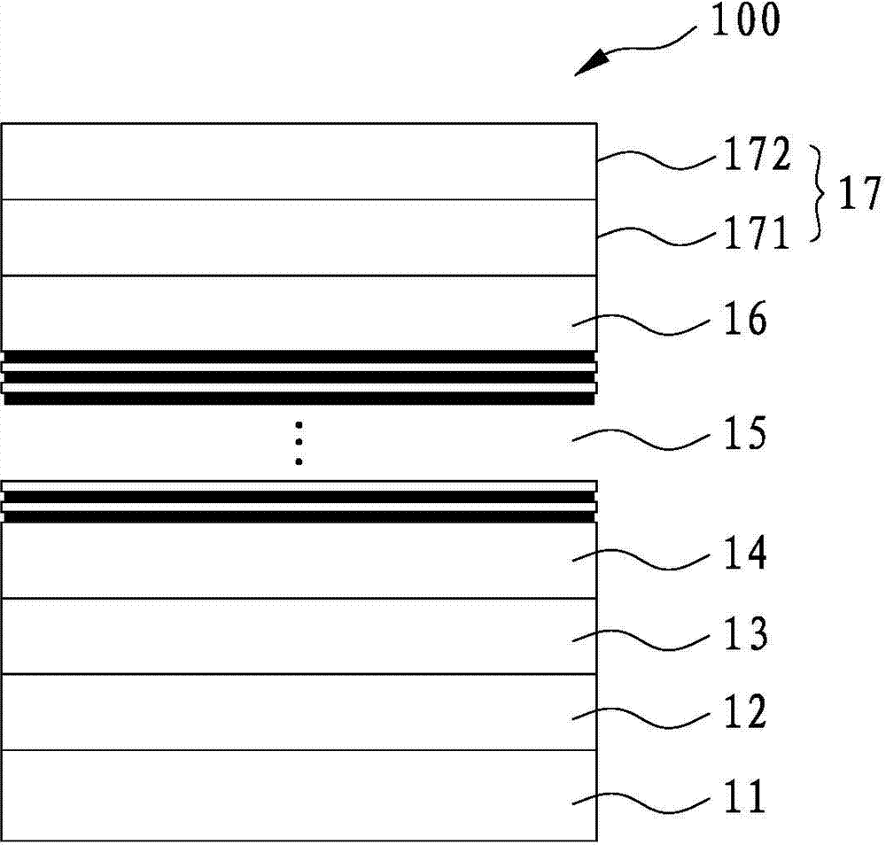
[0059] Such as figure 1 As shown in the first embodiment 100 of the epitaxial structure of a near-infrared light-emitting diode disclosed in the present invention, the cut-off layer 12, the first-type current spreading layer 13, the first-type confinement layer 14, the first-type confinement layer 14, and the The active layer 15 , the second-type confinement layer 16 , the second-type current spreading layer 17 , and the second-type current spreading layer 17 are composed of a first component 171 and a second component 172 .
[0060] Wherein, the corrosion stop layer 12 is (Al 0.1 Ga 0.9 ) 0.5 In 0.5 Composed of P material; the active layer 15 adopts the quantum well structure of AlGaInAs / AlGaAs, the logarithm of the quantum well is 7 pairs, and the light emission wavelength is 850nm; Layer 14 and the second-type confinement layer 16 are made of AlGaAs material, and the first component 171 of the second-type current spreading layer is made of Al 0.1 Ga 0.9 As III-V compo...
Embodiment 2
[0064] Such as Figure 4 Shown is the second embodiment 200 of the epitaxial structure of a near-infrared light-emitting diode disclosed by the present invention. On the GaAs substrate 21, the first-type current spreading layer 22, the first-type confinement layer 23, the active layer 24, the second The second-type confinement layer 25 , the second-type current spreading layer 26 , and the second-type current spreading layer 26 are composed of a first component 261 and a second component 262 .
[0065] Among them, the active layer 24 adopts the quantum well structure of AlGaInAs / AlGaAs, the logarithm of the quantum wells is 3 pairs, and the light emission wavelength is 850nm; the material of the first-type current spreading layer 22 is AlGaInP III-V compound, and the thickness is 8.5 μm , the first-type confinement layer 23 and the second-type confinement layer 25 are made of AlGaInP III-V compound, and the first component 261 of the second-type current spreading layer 26 is m...
PUM
| Property | Measurement | Unit |
|---|---|---|
| Luminous wavelength | aaaaa | aaaaa |
| Thickness | aaaaa | aaaaa |
| Thickness | aaaaa | aaaaa |
Abstract
Description
Claims
Application Information
 - R&D
- Intellectual Property
- Life Sciences
- Materials
- Tech Scout
- Unparalleled Data Quality
- Higher Quality Content
- 60% Fewer Hallucinations
Browse by: Latest US Patents, China's latest patents, Technical Efficacy Thesaurus, Application Domain, Technology Topic, Popular Technical Reports.
© 2025 PatSnap. All rights reserved.Legal|Privacy policy|Modern Slavery Act Transparency Statement|Sitemap|About US| Contact US: help@patsnap.com