Method for manufacturing fin field effect tube

A technology of a fin field effect transistor and a manufacturing method, which is applied in the manufacture of semiconductor/solid state devices, electrical components, semiconductor devices, etc., can solve the problem that the Fin step engraving process is not easy to control, affects the height and shape of fins, and has a high aspect ratio concave Difficulties in trench etching and filling processes

Active Publication Date: 2014-01-15
SEMICON MFG INT (SHANGHAI) CORP
View PDF4 Cites 16 Cited by
  • Summary
  • Abstract
  • Description
  • Claims
  • Application Information

AI Technical Summary

Problems solved by technology

[0023] In view of this, the technical problem solved by the present invention is: in the process of manufacturing STI of FinFET, the etching and filling process of high aspec

Method used


Image

  • Method for manufacturing fin field effect tube
  • Method for manufacturing fin field effect tube
  • Method for manufacturing fin field effect tube

Examples


specific Embodiment 1

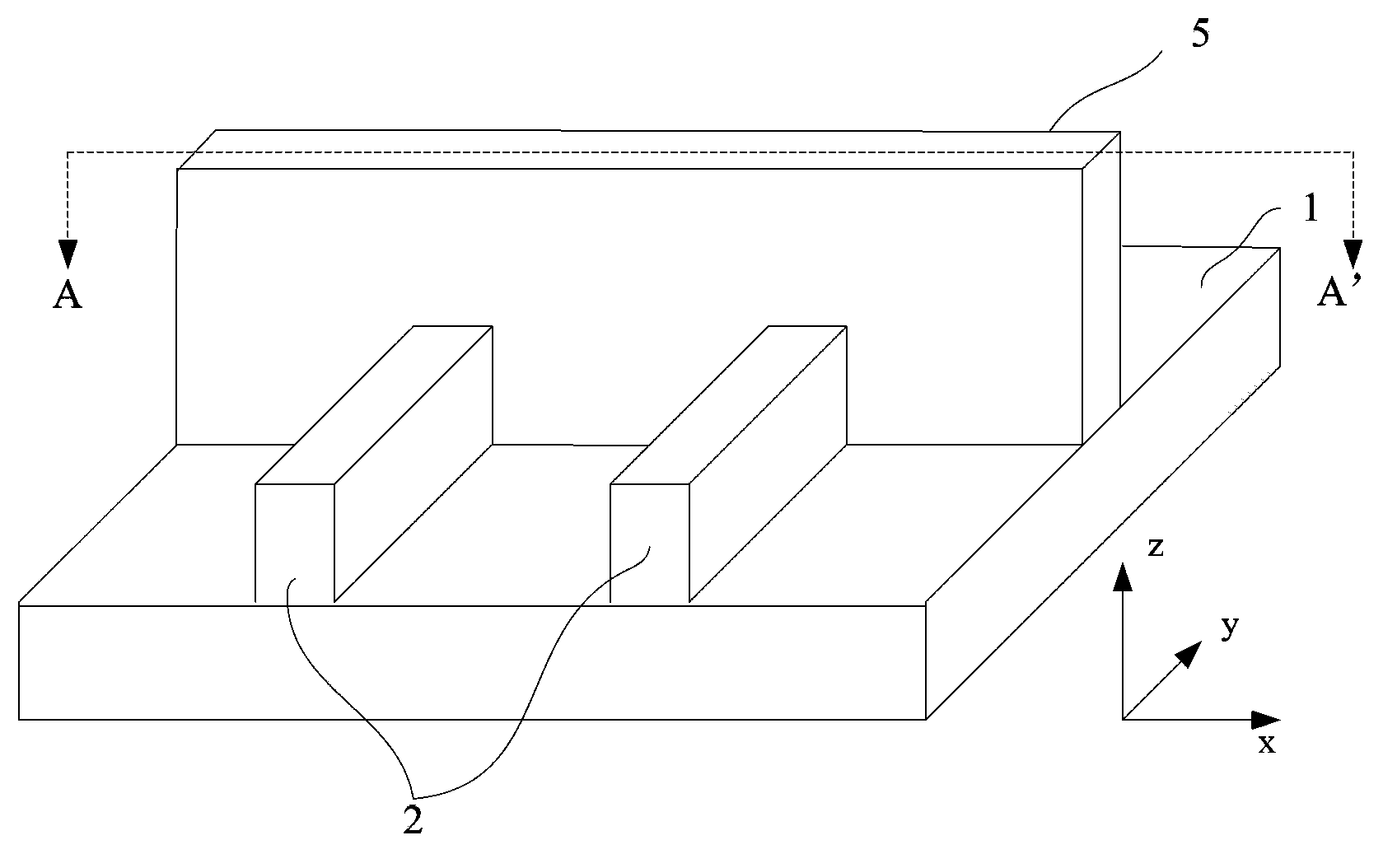
[0055] combine Figure 10~16 Illustrate the present invention as Figure 9 The specific steps for the fabrication of the FinFET shown are as follows:

[0056] Step 901, Figure 10 Schematic diagram of the cross-sectional structure of the FinFET manufacturing step 901 of the present invention, such as Figure 10 As shown, a silicon germanium (SiGe) layer 101 and a silicon (Si) layer 102 are epitaxially grown on the wafer device surface of the semiconductor substrate 100 in sequence;

[0057] In this step, a wafer with a semiconductor substrate 100 is provided, and the semiconductor substrate 100 is bulk silicon or silicon-on-insulator SOI; the thickness of the epitaxially grown SiGe layer 101 ranges from 5 nanometers (nm) to 50 nanometers, for example: 5 nanometers , 20 nanometers or 50 nanometers; the thickness range of the epitaxial growth Si layer 102 is 10 nanometers to 100 nanometers, for example: 10 nanometers, 50 nanometers or 100 nanometers; the thickness of the SiGe...

specific Embodiment 2

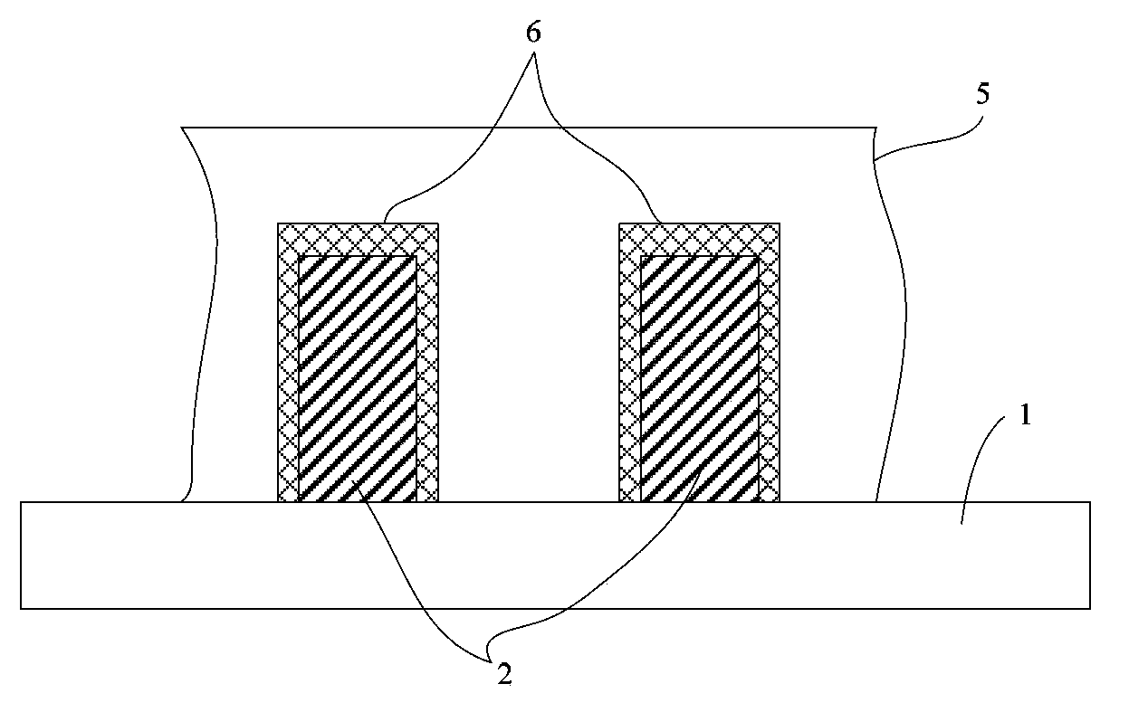
[0075] combine Figure 18~24 In the present invention, such as Figure 17 The specific steps of the FinFET fabrication shown are as follows:

[0076] Step 1001, Figure 18 Schematic diagram of the cross-sectional structure of the FinFET manufacturing step 1001 of the present invention, such as Figure 18 As shown, a silicon germanium (SiGe) layer 101 and a silicon (Si) layer 102 are epitaxially grown on the wafer device surface of the semiconductor substrate 100 in sequence;

[0077] In this step, a wafer with a semiconductor substrate 100 is provided, and the semiconductor substrate 100 is bulk silicon or silicon-on-insulator SOI; the thickness of the epitaxially grown SiGe layer 101 ranges from 5 nanometers (nm) to 50 nanometers, for example: 5 nanometers , 20 nanometers or 50 nanometers; the thickness range of the epitaxial growth Si layer 102 is 10 nanometers (nm) to 100 nanometers, for example: 10 nanometers, 50 nanometers or 100 nanometers; the SiGe layer 101 and the ...


PUM

PropertyMeasurementUnit
Thicknessaaaaaaaaaa
Thicknessaaaaaaaaaa

Abstract

The invention discloses a method for manufacturing a fin field effect tube (Fin FET). According to the method for manufacturing the Fin FET, the height of a formed Fin is accurately controlled by means of epitaxial growth of a germanium-silicon layer and a silicon layer and the high-etching selection ratios of the germanium-silicon layer to a semiconductor substrate and the silicon layer, the parts, below the source electrode and the drain electrode of the Fin, of the silicon layer are removed by means of selective etching after a gate structure and lateral walls which surround the Fin are formed and the source electrode and the drain electrode are infused, and finally source electrode isolation and drain electrode isolation are formed in a groove by means of the Flowable CVD silicon dioxide method. The method for manufacturing the Fin FET has the advantages that on one hand, the depth of the groove in the semiconductor substrate is prevented from being too large, the groove is filled with dielectric media which serve as STI, the Fin can be formed without the need of re-etching of part of the dielectric media, and the height of the Fin is controlled accurately by means of the epitaxial growth of the Si layer; on the other hand, silicon dioxide is adopted to serve as a medium buried layer, a leakage channel of the source electrode and the drain electrode is cut off, and then leakage currents are reduced.

Description

technical field [0001] The invention relates to a manufacturing technology of a semiconductor device, in particular to a manufacturing method of a Fin Field Effect Transistor (FinFET). Background technique [0002] With the development of semiconductor technology, the characteristic size of the metal oxide semiconductor transistor (MOSFET), which is one of the signs of its development, has been continuously scaled down in accordance with Moore's law. Performance and power consumption also continue to improve. In order to further increase the speed of semiconductor devices, three-dimensional (3D) structure or non-planar (non-planar) structure MOSFETs, which are different from traditional planar MOSFETs, have been proposed in recent years, that is, horizontal multi-sided gate structures and vertical multi-sided gate structures have been developed. three-dimensional structure. [0003] The three-dimensional multi-plane gate MOSFET can be intuitively divided into horizontal mu...

Claims


Application Information

Patent Timeline
IPC IPC(8): H01L21/28H01L21/762H01L21/336
CPCH01L21/0274H01L21/31111H01L29/66795
Inventor 卜伟海
Owner SEMICON MFG INT (SHANGHAI) CORP
Why Eureka
Try Eureka