Semiconductor element and manufacturing method thereof

A technology of semiconductors and manufacturing methods, which is applied in the field of semiconductor elements with oxide semiconductor layers and their manufacturing, can solve problems affecting product electrical reliability, affecting product structure reliability, and increasing leakage current, and achieve optimal structure and electrical reliability. reliability, reduce side erosion, and simplify the manufacturing process

Active Publication Date: 2014-02-12
HANNSTAR DISPLAY CORPORATION
View PDF5 Cites 5 Cited by
  • Summary
  • Abstract
  • Description
  • Claims
  • Application Information

AI Technical Summary

Problems solved by technology

Furthermore, when the source and drain are subsequently formed, the etchant will cause side etching on the side of the exposed oxide semiconductor layer, which will affect the structural reliability of subsequent products.
In addition, the metal layer defining the source and drain is in contact with the side of the oxide semiconductor layer during deposition. If it is not etched clean in the subsequent etching steps, there will be a risk of increased leakage current or conduction, which will affect the product. electrical reliability

Method used


Image

  • Semiconductor element and manufacturing method thereof
  • Semiconductor element and manufacturing method thereof
  • Semiconductor element and manufacturing method thereof

Examples


Embodiment Construction

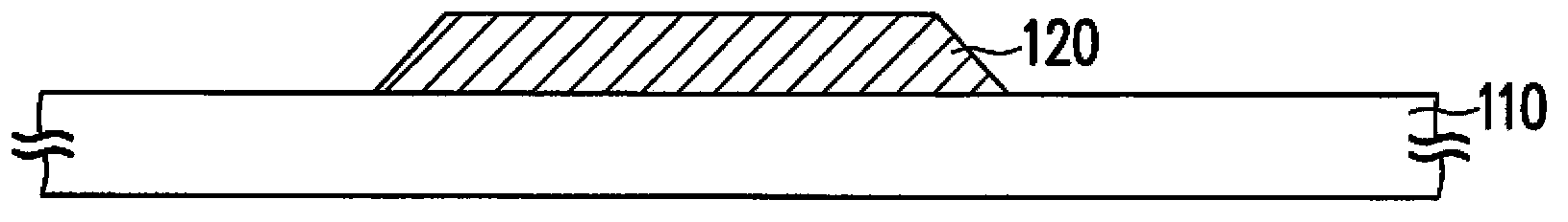
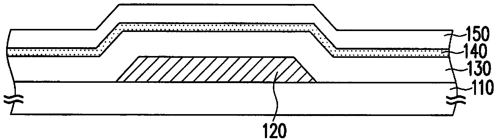
[0040] Figure 1A to Figure 1H It is a schematic cross-sectional view of a manufacturing method of a semiconductor element according to an embodiment of the present invention. Please refer to Figure 1A According to the manufacturing method of the semiconductor device of this embodiment, first, a gate 120 is formed on a substrate 110, wherein the gate 120 is disposed on the substrate 110 and exposes part of the substrate 110, and the material of the substrate 110 includes glass or plastic , without limitation here. Here, the gate 120 is formed by first forming a gate metal layer (not shown) on the substrate 110 , and defining the gate 120 by performing a first photomask step.

[0041] Next, please refer to Figure 1B, sequentially forming a gate insulating layer 130 , an oxide semiconductor layer 140 and an etch stop layer 150 stacked on the substrate 110 . The gate insulating layer 130 covers the gate 120 and part of the substrate 110 . Here, the oxide semiconductor layer...


PUM


Abstract

Provided are a semiconductor element and a manufacturing method thereof. The manufacturing method of the semiconductor element comprises the steps of sequentially forming a gate electrode, a gate insulating layer, an oxide semiconductor layer and an etching stop layer on a substrate, wherein the etching stop layer is provided with two contact openings enabling a part of the oxide semiconductor layer to expose; forming a metal layer on the etching stop layer, wherein the metal layer is connected with the oxide semiconductor layer through the contact openings; forming a partly-adjustable type patterning photoresist layer on the metal layer; using the partly-adjustable type patterning photoresist layer as a mask to remove the metal layer being exposed out of the partly-adjustable type patterning photoresist layer and the etching stop layer under the metal layer; decreasing the thickness of the partly-adjustable type patterning photoresist layer till a second portion is completely removed and forming a patterning photoresist layer; using the patterning photoresist layer as a mask to remove the metal layer being exposed out of the patterning photoresist layer and the oxide semiconductor layer and defining a source electrode, a drain electrode and a channel region; removing the patterning photoresist layer.

Description

technical field [0001] The present invention relates to a semiconductor element and its manufacturing method, and in particular to a semiconductor element with an oxide semiconductor layer and its manufacturing method. Background technique [0002] Recently, the awareness of environmental protection has risen, and liquid crystal display panels (Liquid crystal display panels) with superior characteristics such as low power consumption, good space utilization efficiency, no radiation, and high image quality have become the mainstream of the market. In the past, liquid crystal display panels mostly used amorphous silicon (a-Si) thin film transistors or low-temperature polysilicon (Low-temperature polysilicon, LTPS) thin film transistors as switching elements of each pixel structure. However, in recent years, studies have pointed out that: compared with amorphous silicon thin film transistors, oxide semiconductor thin film transistors have higher carrier mobility (mobility); and...

Claims


Application Information

Patent Timeline
Patent Type & Authority Applications(China)
IPC IPC(8): H01L21/335H01L21/027
CPCH01L29/66742H01L29/7869H01L21/027H01L29/66969H01L21/0274
Inventor 张荣芳张民杰
Owner HANNSTAR DISPLAY CORPORATION
Why Eureka
Try Eureka