Supercharge Your Innovation With Domain-Expert AI Agents!

SiC single crystal and method for manufacturing same, SiC wafer, and semiconductor device

一种单晶、生长晶体的技术,应用在半导体器件、半导体/固态器件制造、晶体生长等方向,能够解决不能避免叠层缺陷、难以切出大直径的衬底、偏离角大等问题

Active Publication Date: 2014-02-12
KK TOYOTA CHUO KENKYUSHO +2
View PDF6 Cites 5 Cited by
  • Summary
  • Abstract
  • Description
  • Claims
  • Application Information

AI Technical Summary

Problems solved by technology

[0025] (2) the occurrence of lamination defects during a-plane growth cannot be avoided; and
[0031] (3) When the deviation angle relative to the (000-1) C plane direction is too large, it is easy to produce a mixture of polytypes and produce a large number of crystal defects
Therefore, the final yield when cutting out {0001} plane substrates decreases, and it is difficult to cut out large-diameter substrates

Method used


Image

  • SiC single crystal and method for manufacturing same, SiC wafer, and semiconductor device
  • SiC single crystal and method for manufacturing same, SiC wafer, and semiconductor device
  • SiC single crystal and method for manufacturing same, SiC wafer, and semiconductor device

Examples


Embodiment Construction

[0079] Hereinafter, preferred embodiments of the present invention will be described in detail.

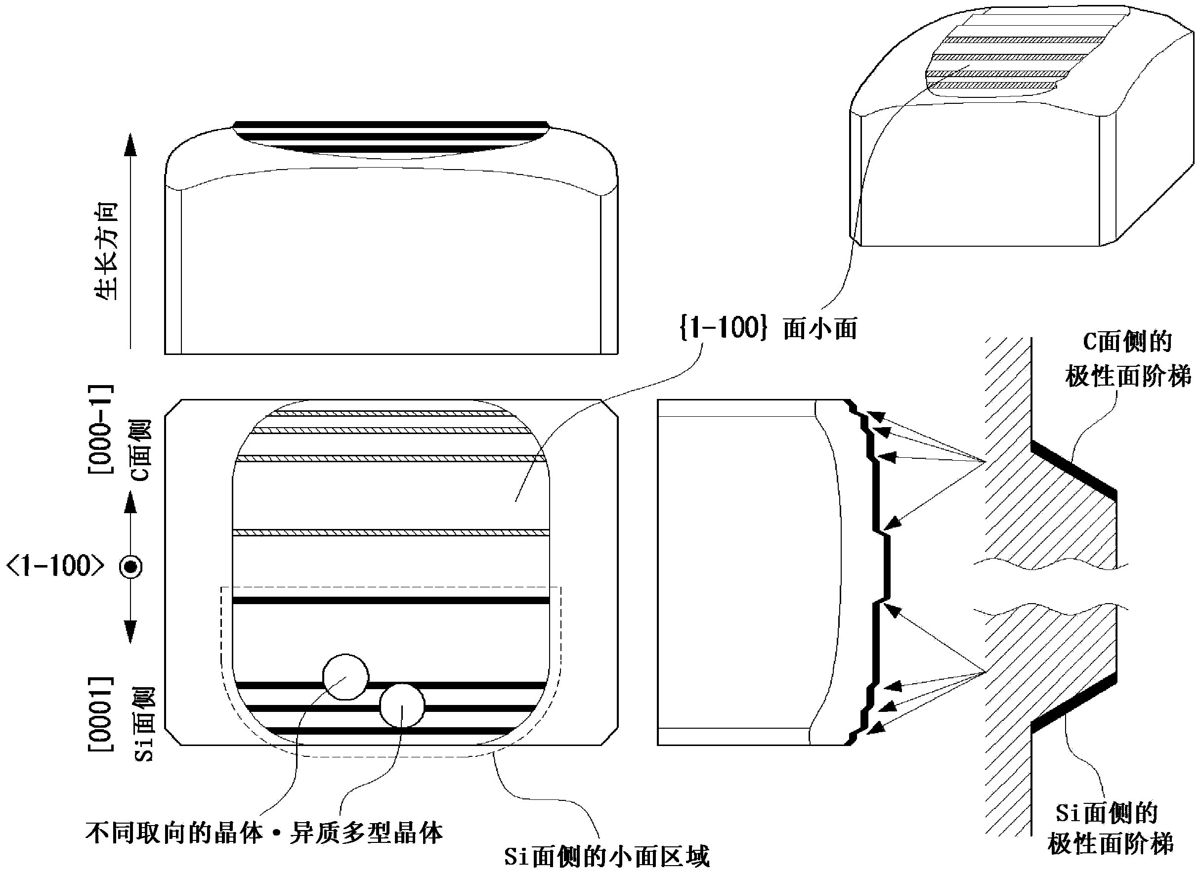
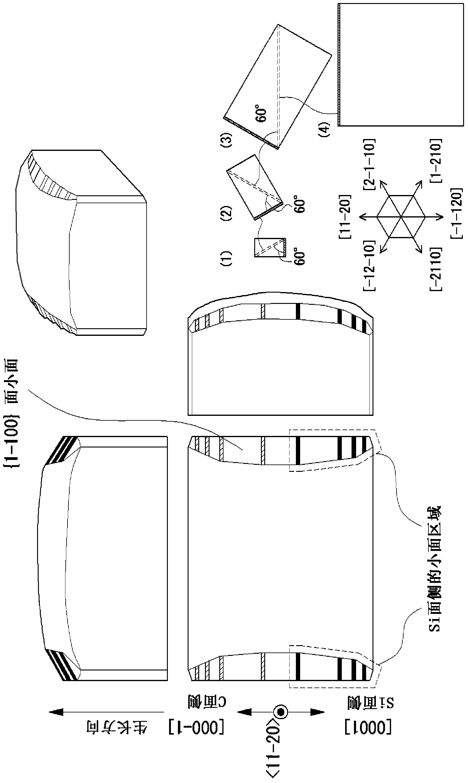
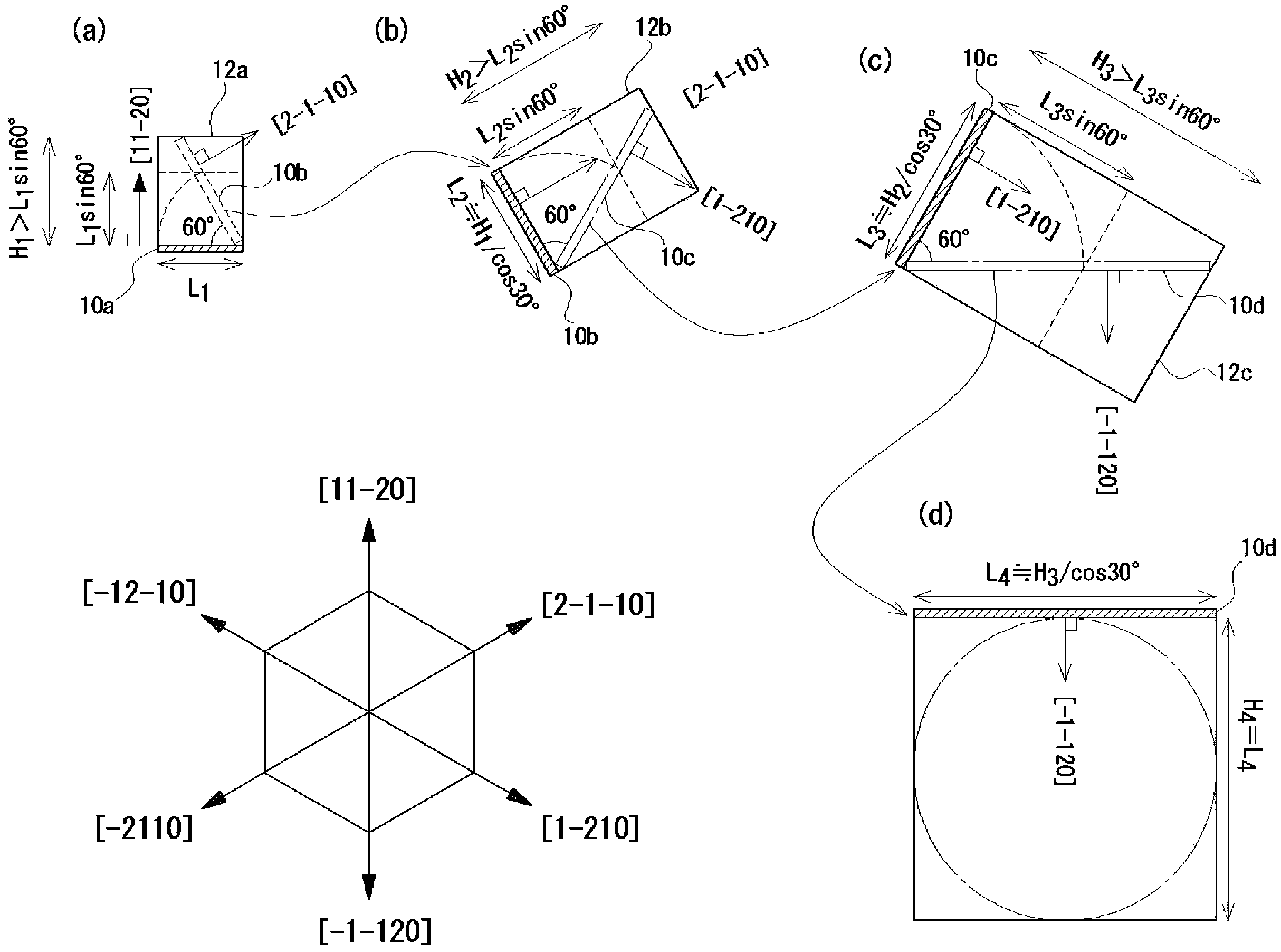
[0080] [1. Definition of terms]

[0081] [1.1.a surface growth]

[0082] The term "growth plane" means a plane for growing a seed crystal of a new single crystal composed of SiC.

[0083] The term "a-plane growth" means growing a new single crystal composed of SiC by using a plane whose off angle from the {11-20} plane or {1-100} plane is within a predetermined range as a growth plane.

[0084] The term "{11-20} plane growth (or growth)" refers to growing a new single cell composed of SiC by using a plane whose off angle from the {11-20} plane is within a predetermined range as a growth plane. crystal.

[0085] The term "{1-100} plane growth (or growth)" refers to growing a new single cell made of SiC by using a plane whose off angle from the {1-100} plane is within a predetermined range as a growth plane. crystal.


PUM

PropertyMeasurementUnit
diameteraaaaaaaaaa
diameteraaaaaaaaaa

Abstract

When a SiC single crystal having a large {0001} face diameter is manufactured by repeating an a-face growth, the SiC single crystal is grown on the a-face so that the ratio (Sfcaet) of the area (S1) of a Si-face side facet region to the total area (S2) of the growth face (Sfcaet = S1 × 100 / S2) is maintained at 20 % or less. It is preferable that the a-face growth is performed by a {11-20} face selection growth method in which the a-face growth is repeated in approximately 60° or 120° different direction with reference to the {11-20} face or an alternate growth method in which {11-20} face growth and {1-100} face growth are alternately repeated.

Description

technical field [0001] The invention relates to SiC single crystal and its manufacturing method, SiC wafer and semiconductor device. More specifically, the present invention relates to a SiC single crystal containing few crystal masses of different orientations or few heterogeneous polytype crystal masses, a method of manufacturing the same, and SiC wafers and semiconductor devices cut out from the SiC single crystal. Background technique [0002] In SiC (silicon carbide), a high-temperature type (α type) having a hexagonal crystal structure and a low-temperature type (β type) having a cubic crystal structure are known. Compared with Si, SiC is characterized by high heat resistance, wide bandgap, and high dielectric breakdown electric field strength. For this reason, semiconductors including SiC single crystals are expected to be candidate materials for next-generation power devices replacing Si semiconductors. In particular, α-type SiC has a wider band gap than β-type SiC...

Claims


Application Information

Patent Timeline
Patent Type & Authority Applications(China)
IPC IPC(8): C30B29/36H01L21/203
CPCC30B23/00C30B29/36C30B23/005H01L21/02433H01L21/02529H01L21/02609C30B23/025H01L21/02378H01L21/0243H01L21/02587H01L29/1608Y10T428/21
Inventor 郡司岛造重藤启辅浦上泰山田正德安达步小林正和
Owner KK TOYOTA CHUO KENKYUSHO
Features
  • R&D
  • Intellectual Property
  • Life Sciences
  • Materials
  • Tech Scout
  • Unparalleled Data Quality
  • Higher Quality Content
  • 60% Fewer Hallucinations
Learn More