Tunneling field effect floating gate transistor and manufacturing method thereof

A floating gate transistor and tunneling field effect technology, which is applied in the field of device manufacturing, can solve problems such as data loss and hinder the escape of floating gate electrons, and achieve the effects of improved data storage time, wide application, and low production cost

Inactive Publication Date: 2014-02-19
SUZHOU ZHIQUAN ELECTRONICS TECH CO LTD
View PDF5 Cites 7 Cited by
  • Summary
  • Abstract
  • Description
  • Claims
  • Application Information

AI Technical Summary

Problems solved by technology

[0006] The purpose of the present invention is to provide a new tunneling field for the problem that the bandgap width of the silicon-based P-N junction diode is only 1.1eV, and the data stored in the tunneling field effect semi-floating gate transistor is easily lost due to the escape of electrons. Effect floating gate transistor and its manufacturing method, which forms a new floating gate transistor by depositing a thin gate oxide layer between the floating gate region and the p-n diode region of the substrate, and can effectively use silicon oxide with a high band gap to prevent floating Escape of electrons stored in the gate

Method used


Image

  • Tunneling field effect floating gate transistor and manufacturing method thereof
  • Tunneling field effect floating gate transistor and manufacturing method thereof
  • Tunneling field effect floating gate transistor and manufacturing method thereof

Examples


Embodiment Construction

[0041] The following description is a preferred embodiment embodying the principles of the present invention. It should be noted that the accompanying drawings are schematic diagrams of idealized embodiments of the present invention, and the shapes and sizes shown in each part do not represent actual shapes and sizes. But it still fully reflects the mutual position between the area and each part, especially the up-down and adjacent relationship between components.

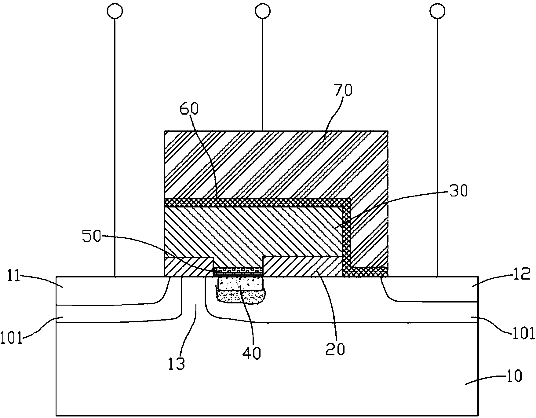
[0042] See figure 1 As shown in the cross-sectional view along the channel direction, the tunneling field effect floating gate transistor of the present invention includes the following parts:

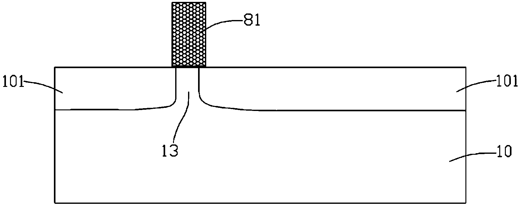
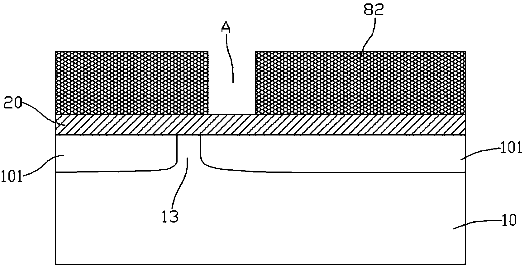
[0043] a semiconductor substrate 10 with a first doping type;

[0044] A source 11 and a drain 12 having a second doping type formed on the semiconductor substrate 10;

[0045] a channel region 13 formed in the semiconductor substrate 10 between the source electrode 11 and the drain electrode 12;

[0046] A first insulat...


PUM


Abstract

The invention discloses a tunneling field effect floating gate transistor which comprises a semiconductor substrate in a first doping type, a source electrode in a second doping type, a drain electrode in a second doping type, a channel area, a first layer insulating film, a conductive floating gate area, a p-n junction diode, a thin gate-oxide area, a second layer insulating film and a control grid electrode. The source electrode and the drain electrode are formed on the semiconductor substrate, the channel area is formed in the semiconductor substrate between the source electrode and the drain electrode, the first layer insulating film covering the whole channel area is formed on the semiconductor substrate, the conductive floating gate area serving as a charge storing node is formed on the first layer insulating film, the p-n junction diode is formed between the floating gate area and the channel area, the thin gate-oxide layer is formed between the p-n junction diode and the floating gate area, the second layer insulating film covers the floating gate area, and the control grid electrode is formed on the second layer insulating film. The thin gate-oxide layer is deposited between the floating gate area and the substrate p-n junction diode to form the new float gate transistor, so that silicon oxide with the high forbidden bandwidth is effectively utilized to block electronic escape stored in the floating gate.

Description

Technical field: [0001] The invention relates to the technical field of semiconductor devices, in particular to a low-power semiconductor device formed by combining an ultra-thin gate oxide with a P-N junction diode on the basis of a tunneling field effect transistor, and a manufacturing method of the device . Background technique: [0002] Metal-oxide-silicon field-effect transistors (MOSFETs) are widely used in various electronic products. With the development of integrated circuit technology, the size of MOSFETs is getting smaller and smaller, and the density of transistors on the unit array is getting higher and higher. , but the leakage phenomenon caused by the ensuing short-communication effect is becoming more and more obvious. How to reduce the power consumption of convenient devices has become a research hotspot in the field of semiconductor technology. [0003] Corresponding to the development of MOSFET, there is non-volatile memory. Non-volatile memory means that...

Claims


Application Information

Patent Timeline
Patent Type & Authority Applications(China)
IPC IPC(8): H01L29/78H01L21/336H01L29/06
CPCH01L29/788H01L29/1029H01L29/66825
Inventor 刘开锋刘红元其他发明人请求不公开姓名
Owner SUZHOU ZHIQUAN ELECTRONICS TECH CO LTD
Why Eureka
Try Eureka