Line structure and manufacturing method thereof

A technology of circuit structure and production method, which is applied in the direction of multilayer circuit manufacturing, printed circuit components, and electrical connection formation of printed components, can solve problems such as signal line interference and affect signal transmission integrity, and reduce electromagnetic wave interference. The effect of signal transmission quality and reduction of crosstalk noise interference

Active Publication Date: 2014-02-19
UNIMICRON TECH CORP
View PDF5 Cites 3 Cited by
  • Summary
  • Abstract
  • Description
  • Claims
  • Application Information

AI Technical Summary

Problems solved by technology

However, although there are components or protectors on the upper and lower sides of the signal line to avoid the spread of electromagnetic waves, the left and right sides of the signal line are essentially open spaces
Therefore, electromagnetic waves are easy to interfere with the signal transmission of the signal line from the left and right sides of the signal line, which means that the signal line is susceptible to electromagnetic wave interference, which in turn affects the integrity of signal transmission

Method used


Image

  • Line structure and manufacturing method thereof
  • Line structure and manufacturing method thereof
  • Line structure and manufacturing method thereof

Examples


Embodiment Construction

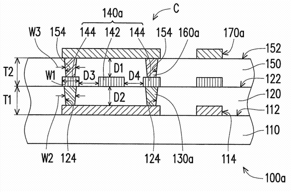
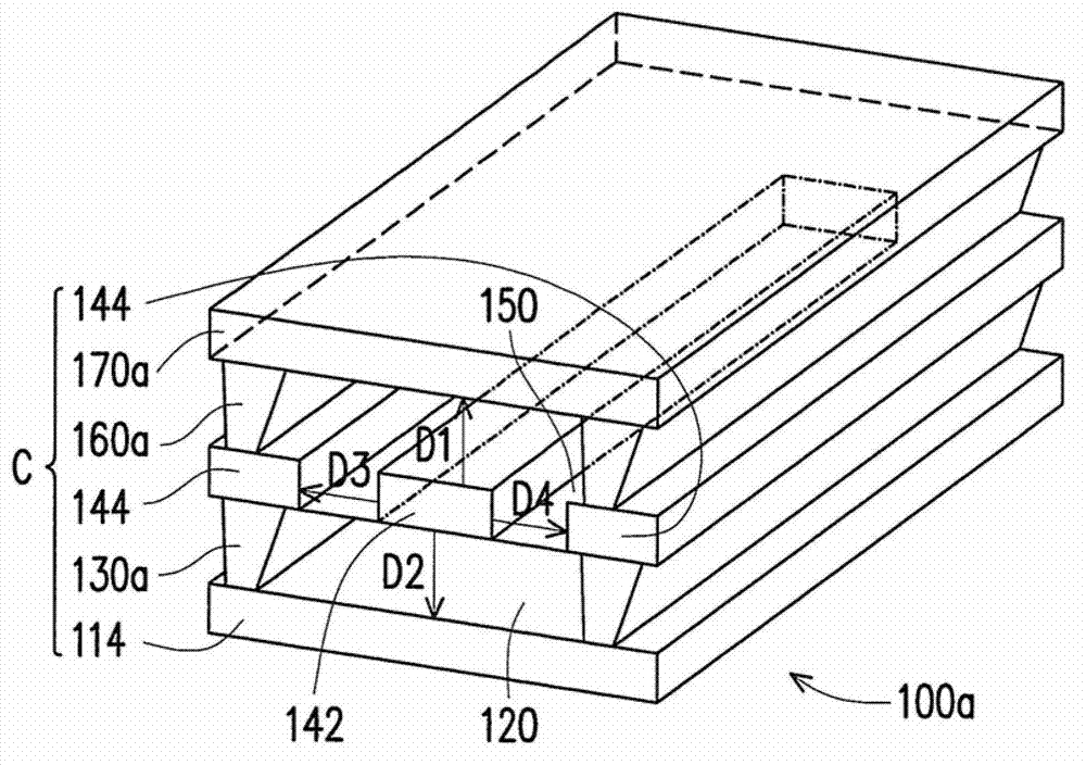
[0048]Figure 1A It is a schematic cross-sectional view of a circuit structure according to an embodiment of the present invention. Figure 1B for Figure 1A A partial three-dimensional schematic diagram of the line structure. Please also refer to Figure 1A and Figure 1B , in this embodiment, the wiring structure 100a includes an inner wiring layer 110, a first dielectric layer 120, a first conductive material layer 130a, a second conductive layer 140a, a second dielectric layer 150, a The second conductive material layer 160a and a third conductive layer 170a.

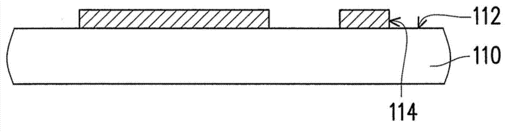
[0049] In detail, the inner circuit layer 110 has an upper surface 112 and a first conductive layer 114 disposed on the upper surface 112 . The first dielectric layer 120 is disposed on the inner circuit layer 110 and covers the upper surface 112 and the first conductive layer 114 . The first dielectric layer 120 has a first surface 122 and a plurality of first circuit trenches 124 extending from the first surface...


PUM


Abstract

The invention discloses a line structure and a manufacturing method thereof. The line structure comprises an inner line layer, a first dielectric layer, a first conductive material layer, a second conductive layer, a second dielectric layer, a second conductive material layer and a third conductive layer. The first dielectric layer covers a first conductive layer of the inner line layer and is provided with a first surface and multiple first line trenches; the first conductive material layer is configured in the first line trenches; the second conductive layer is configured on the first surface and comprises a signal line and at least two reference lines; the second dielectric layer covers the first surface and the second conductive layer and is provided with a second surface and multiple second line trenches; the width of each first line trench and the width of each second line trench are smaller than the line width of each reference line; the second conductive material layer is configured in the second line trenches; and the third conductive material layer is configured on the second surface.

Description

technical field [0001] The invention relates to a circuit structure and a manufacturing method thereof, and in particular to a circuit structure with electromagnetic shielding effect and a manufacturing method thereof. Background technique [0002] With the progress of the printed circuit board (PCB) manufacturing technology, the size of the printed circuit board itself is getting smaller and smaller. Due to many design requirements, not only the number of circuit components arranged on the printed circuit board must be more and more, but also the signal transmission speed between the circuit components must be faster and faster. However, if a large number of circuit components are laid out in a limited circuit board area, the spacing between signal lines must be reduced, resulting in crosstalk between these signal lines, which will affect the Transmission quality. If the pitch of these signal lines is increased, the area where the actual circuit layout can be carried out ...

Claims


Application Information

Patent Timeline
Patent Type & Authority Applications(China)
IPC IPC(8): H05K1/02H05K1/11H05K3/46H05K3/42
Inventor 黄尚峰余丞博郑人齐
Owner UNIMICRON TECH CORP
Why Eureka
Try Eureka