Mixed-potential type NO2 sensor with mesh-strip structured YSZ (yttria-stabilized zirconia) substrate serving as conductive layer and preparation method for mixed-potential type NO2 sensor
A technology of mixed potential type and conductive layer, which is applied in the field of mixed potential type NO2 sensor and its preparation, can solve the problem of uncontrollable surface morphology and achieve good thermal and chemical stability, shape and surface area controllable Effect
- Summary
- Abstract
- Description
- Claims
- Application Information
AI Technical Summary
Problems solved by technology
Method used
Image
Examples
Embodiment 1
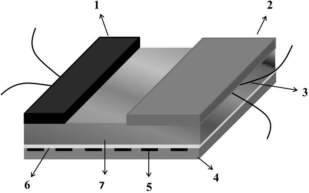
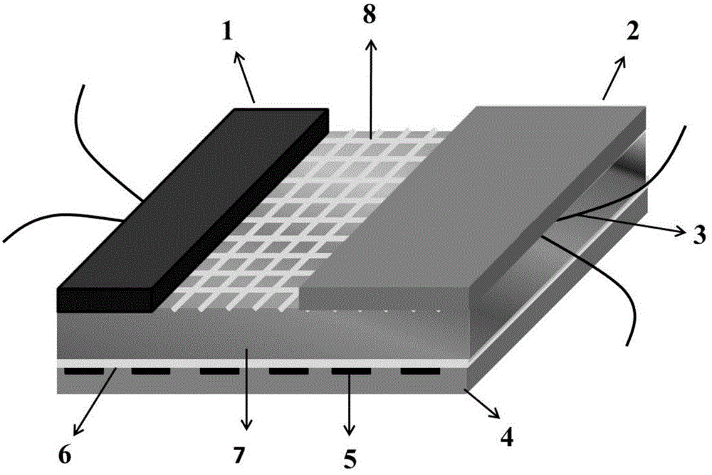
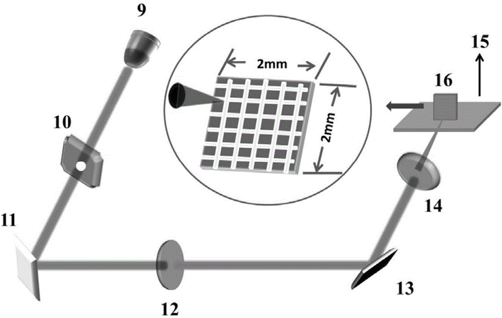
[0051] The YSZ substrate is laser processed, the horizontal and vertical stripe spacing is 240 μm, and the depth is 10 μm. The width of a single stripe is 50 μm. Other manufacturing processes are the same as the comparative example.
[0052] Table 1 lists the devices made of unprocessed YSZ and laser-processed YSZ substrates with a stripe spacing of 240 μm at different concentrations of NO 2 The difference (ΔV) between the electromotive force in the atmosphere and the electromotive force in the air varies with NO 2 It can be seen from the table that the sensitivity of the device made of the laser-processed YSZ substrate with a stripe spacing of 240 μm has improved, but the change is not much.
[0053] Table 1. The ΔEMF of devices fabricated on unprocessed YSZ and laser-processed YSZ substrates with a stripe spacing of 240 μm versus NO 2 change in concentration
[0054]
Embodiment 2
[0056] The YSZ substrate was processed by laser, the horizontal and vertical stripe spacing was 130 μm, the depth was 10 μm, and the width of a single stripe was 50 μm. Other manufacturing processes were the same as those of the comparative example.
[0057] Table 2 lists the devices made of unprocessed YSZ and laser-processed YSZ substrates with a stripe spacing of 50 μm at different concentrations of NO 2 The difference (ΔV) between the electromotive force in the atmosphere and the electromotive force in the air varies with NO 2 It can be seen from the table that the sensitivity of the device made of the laser-processed YSZ substrate with a stripe spacing of 50 μm has been greatly improved.
[0058] Table 2. ΔEMF of devices fabricated on unprocessed YSZ and laser-processed YSZ substrates with a stripe spacing of 130 μm versus NO 2 change in concentration
[0059]
[0060]
PUM
| Property | Measurement | Unit |
|---|---|---|
| depth | aaaaa | aaaaa |
| width | aaaaa | aaaaa |
| wavelength | aaaaa | aaaaa |
Abstract
Description
Claims
Application Information


