Method for directly extracting small-signal model parameters of III-V MOSFET

A small signal model, III-V technology, applied in electrical digital data processing, special data processing applications, instruments, etc., can solve problems such as deviation and deviation from physical meaning

Active Publication Date: 2014-03-05
INST OF MICROELECTRONICS CHINESE ACAD OF SCI
View PDF2 Cites 15 Cited by
  • Summary
  • Abstract
  • Description
  • Claims
  • Application Information

AI Technical Summary

Problems solved by technology

In the literature "A new method for determining the FET small signal equivalent circuit" (IEEE Transaction on Microwave Theory and Techniques, July 1988), Gilles Dambrine et al. described in detail the direct extraction method of GaAs HEMT small signal model parameters, in which the parasitic resistance parameter The extraction is that the device is in a cold state, fully consider the channel resistance under the gate and the equivalent impedance of the Schottky barrier, and use the Z parameter fitting results under 3 different gate current conditions as an additional relationship condition to obtain the parasitic resistance parameter , however, for MOSFET structure devices, due to the insulation of the oxide layer under the gate, such a method is no longer applicable; the intrinsic parameters are calculated by the analytical method to obtain the functional relationship of the intrinsic parameters with respect to frequency, and then the parameters are obtained in the frequency flat region The value obtained in

Method used


Image

  • Method for directly extracting small-signal model parameters of III-V MOSFET
  • Method for directly extracting small-signal model parameters of III-V MOSFET
  • Method for directly extracting small-signal model parameters of III-V MOSFET

Examples


Embodiment Construction

[0065] In order to make the object, technical solution and advantages of the present invention clearer, the present invention will be described in further detail below in conjunction with specific embodiments and with reference to the accompanying drawings.

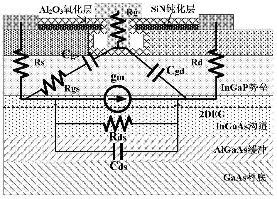
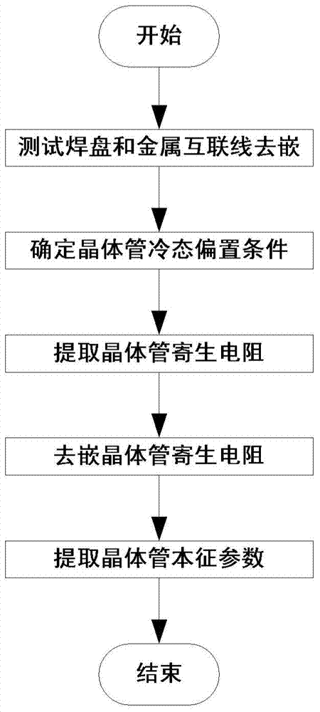
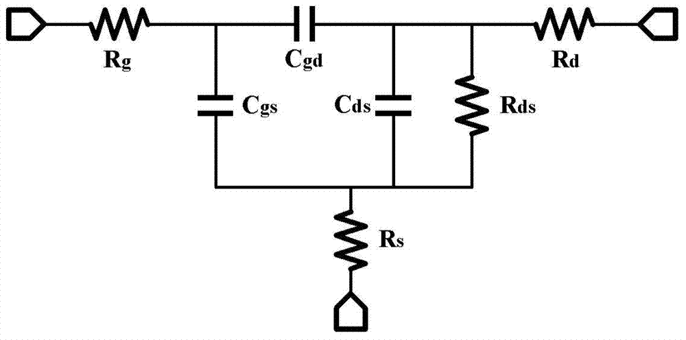
[0066] The method for directly extracting small-signal model parameters of this III-V family MOSFET provided by the present invention is to de-embed through pads and metal interconnection lines, and use transistor DC transfer characteristics and cold-state S parameters to determine the appropriate bias when extracting transistor parasitic resistance. Under this bias condition, the influence of the channel resistance is removed, the parasitic resistance parameters are extracted by linear fitting, and finally the parasitic resistance is de-embedded, and the small-signal model equivalent circuit and curve fitting of the III-V MOSFET are used to extract the characteristic parameters, the method specifically includes the follow...


PUM


Abstract

The invention discloses a method for directly extracting small-signal model parameters of an III-V family MOSFET, and belongs to the technical field of micro-electronics integrated circuits. The method includes the steps of conducting de-embedding through a bonding pad and a metal interconnection line, determining, by means of the transistor direct-current transfer characteristic and a cold state S parameter, a bias condition suitable for extracting a transistor parasitic resistor, then, removing the influences of a channel resistor under the bias condition, conducting linear fitting to extract the parameters of the parasitic resistor, finally, conducting de-embedding on the parasitic resistor, and extracting intrinsic parameters through an equivalent circuit of a small-signal model of the III-V family MOSFET and through linear fitting. The process for directly extracting the small-signal parameters completely conforms to the physical significance of a device, a necessary foundation for the application of the integrated circuit technology is provided, and meanwhile the method has a very good reference function for extraction of small-signal model parameters of other types of devices which are made of novel materials and are of novel structures.

Description

technical field [0001] The present invention relates to the technical field of microelectronic integrated circuits, in particular to a method for directly extracting small-signal model parameters of III-V MOSFETs, which can be used to effectively extract small-signal parameter results of III-V MOSFET type devices for use in device technology Optimization and circuit simulation design. Background technique [0002] At the 11nm technology node and beyond, due to the limitations of the physical properties of silicon materials, silicon-based CMOS technology will face enormous challenges, and high-mobility "non-silicon" materials will be gradually introduced into CMOS technology. III-V compound semiconductor materials have the advantages of high electron mobility, short intrinsic delay time, good radio frequency performance, small gate leakage, low static power consumption, etc., and have become a research hotspot in the current international MOSFET technology. Accurate extracti...

Claims


Application Information

Patent Timeline
IPC IPC(8): G06F17/50
Inventor 刘洪刚刘桂明常虎东
Owner INST OF MICROELECTRONICS CHINESE ACAD OF SCI
Why Eureka
Try Eureka