

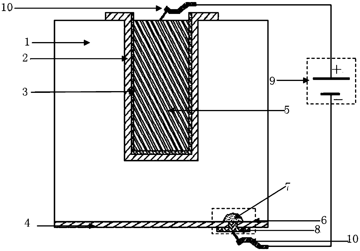
TSV (through silicon via) through hole insulation layer test structure based on SOI (silicon on insulator) substrate
A substrate and test point technology, applied in the field of microelectronics, can solve the problems of increasing the reliability of SOI three-dimensional integrated devices, withstand voltage and leakage tests, effective insulating layers, etc., to avoid economic losses, improve reliability, and reduce costs. Effect
- Summary
- Abstract
- Description
- Claims
- Application Information
AI Technical Summary
Problems solved by technology
Method used
Image

Examples
Embodiment 1
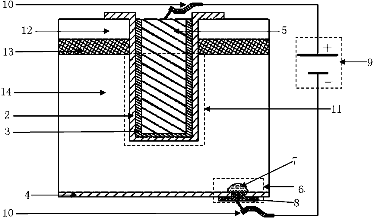
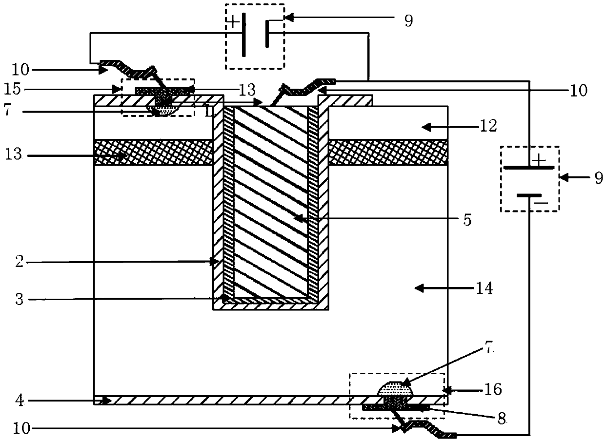
[0014] like image 3 As shown, the SOI wafer substrate is P-type silicon, and the thickness of the buried oxide layer 13 is Top Silicon 12 Thickness The bottom silicon 14 has a thickness of 80 μm, the TSV copper pillar 5 has a diameter of 30 μm, the TSV through-hole insulation layer 2 has a thickness of 0.6 μm, the barrier layer TaN and copper seed 3 have a thickness of 0.4 μm, and the bottom insulation layer 4 of the silicon substrate has a thickness of 1 μm. The No. 2 ohmic contact test point 16 is located on the back side of the underlying silicon 14, wherein the active region 7 of the No. 2 ohmic contact test point 16 is a heavily doped P+ region, and the implantation depth The aluminum metal pad 8 is a square of 5 μm × 5 μm; the first ohmic contact test point 15 is located on the front side of the top layer silicon 12, and the pad 8 is 30 μm away from the center of the TSV through hole, and the first ohmic contact test point 15 has an active area 7 For the heavily do...
Embodiment 2
[0017] like image 3 As shown, the SOI wafer substrate is N-type silicon, and the thickness of the buried oxide layer 13 is Top Silicon 12 Thickness The bottom silicon 14 has a thickness of 80 μm, the TSV copper pillar 5 has a diameter of 25 μm, the TSV through-hole insulation layer 2 has a thickness of 0.4 μm, the barrier layer TaN and copper seed 3 have a thickness of 0.2 μm, and the bottom insulation layer 4 of the silicon substrate has a thickness of 1 μm. The No. 2 ohmic contact test point 16 is located on the back side of the underlying silicon 14, wherein the active region 7 of the No. 2 ohmic contact test point 16 is a heavily doped N-region, and the implantation depth The aluminum metal pad 8 is a square of 8 μm×8 μm; the first ohmic contact test point 15 is located on the front side of the top layer silicon 12, and the pad 8 is 25 μm away from the center of the TSV through hole, and the first ohmic contact test point 15 has an active area 7 For the heavily doped...
PUM
 Abstract
Description
Claims
Application Information