PCB
A PCB board and substrate technology, applied in the field of electronic devices, can solve problems such as difficult tinning and easy oxidation of PCB pads, and achieve the effects of easy tinning, avoiding pollution, and reducing electromagnetic radiation
- Summary
- Abstract
- Description
- Claims
- Application Information
AI Technical Summary
Problems solved by technology
Method used
Image

Examples
Embodiment 1
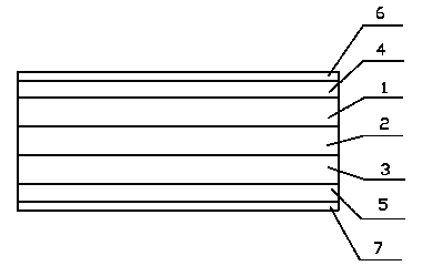
[0020] Embodiment one, such as figure 1 As shown, a PCB board includes first to third substrates, one side of the first substrate 1 is provided with wiring layers, both sides of the second substrate 2 are provided with wiring layers, and the third substrate 3 is provided with wiring layers. A wiring layer is provided on one side, and the first to third substrates are tightly pressed in sequence, wherein, the side of the first substrate 1 without a wiring layer is pressed together with the side of the second substrate 2, and the first substrate 1 is provided with a wiring layer. One side of the wiring layer is provided with the first solder resist layer 4, the side of the third substrate 3 without the wiring layer is pressed against the other side of the second substrate 2, and the side of the third substrate 3 provided with the wiring layer is provided with the second resistance layer. Soldering layer 5; the first solder resist layer 4 and the second solder resist layer 5 are ...
Embodiment 2
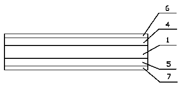
[0026] Embodiment two, such as figure 2 As shown, a PCB board includes a substrate, the substrate is the same as the first to third substrates in Embodiment 1, both sides of the substrate include circuit wiring layers, and a solder resist layer is arranged on the wiring layers , the tin-sprayed layer or the gold-sprayed layer is set on the solder resist layer, the anti-oxidation layer is set on the tin-sprayed layer or the gold-sprayed layer, and the silk screen layer is set on the anti-oxidation layer. The setting of its anti-oxidation layer is the same as that of Embodiment 1.
[0027] The effect and principle of the anti-oxidation layer are as follows:
[0028] Because the gold layer is very thin during the gold plating and immersion gold process of the PCB, the gold layer is too thin, so it is not very dense during the crystallization process, leaving many micropores, which will become the origin of corrosion in the future. As a result, the bottom layer is corroded. Fro...
PUM
 Abstract
Description
Claims
Application Information
 - R&D
- Intellectual Property
- Life Sciences
- Materials
- Tech Scout
- Unparalleled Data Quality
- Higher Quality Content
- 60% Fewer Hallucinations
Browse by: Latest US Patents, China's latest patents, Technical Efficacy Thesaurus, Application Domain, Technology Topic, Popular Technical Reports.
© 2025 PatSnap. All rights reserved.Legal|Privacy policy|Modern Slavery Act Transparency Statement|Sitemap|About US| Contact US: help@patsnap.com