LBJT (Lateral Bipolar Junction Transistor) containing field plate structure

A technology of bipolar transistors and field plates, applied in semiconductor devices, electrical components, circuits, etc., can solve the problems of restricting the blocking voltage and high electric field strength of lateral bipolar transistors, achieve high blocking voltage, improve resistance Cut-off voltage level, enhanced depletion effect

Inactive Publication Date: 2014-03-26
SUZHOU YINGNENG ELECTRONICS TECH
View PDF8 Cites 0 Cited by
  • Summary
  • Abstract
  • Description
  • Claims
  • Application Information

AI Technical Summary

Problems solved by technology

[0005] In power integrated circuits (PICs), lateral bipolar transistors (LBJT) usually adopt a single Sigle RESURF structure with high reverse blocking voltage and low specific on-resistance, but in the collector region Excessive electric field strength exists in the ohmic contact region, which restricts the improvement of the blocking voltage of the lateral bipolar transistor (LBJT)

Method used


Image

  • LBJT (Lateral Bipolar Junction Transistor) containing field plate structure
  • LBJT (Lateral Bipolar Junction Transistor) containing field plate structure
  • LBJT (Lateral Bipolar Junction Transistor) containing field plate structure

Examples


Embodiment 1

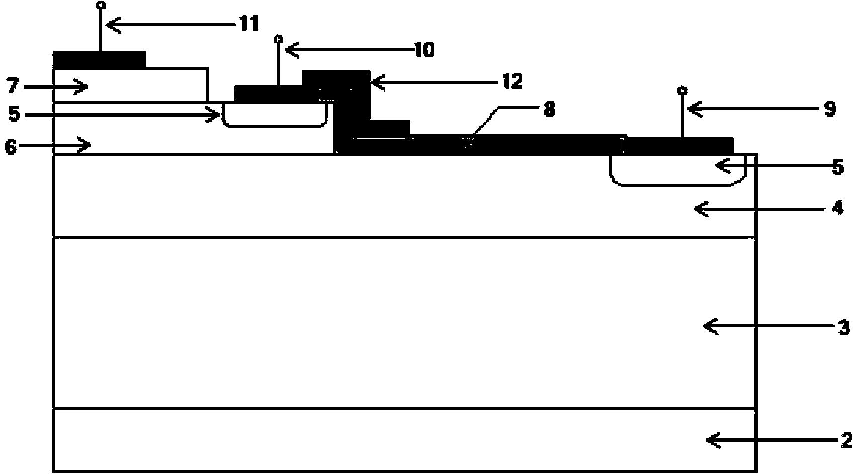
[0030] A specific implementation of the lateral bipolar transistor with field plate structure described in the present invention is given below, see figure 2 As shown, the lateral bipolar transistor with a base field plate structure in this embodiment includes a substrate 2, a buffer zone 3, a collector region 4, a base region 6, and an emitter region 7 from bottom to top, respectively. The ohmic contact region 5 is formed by ion implantation at the upper boundary of the collector region 4 and the base region 6, and metal deposition is performed on the collector region 4, the base region 6, and the emitter region 7 respectively. Metal electrodes are formed in a manner, the emitter 11 is located on the emitter region 7, the collector 9 is located on the ohmic contact region 5 of the collector region 4, and the base 10 is located between the ohmic contact region 5 of the base region 6 Above, a base field plate 12 is provided on the base region 6, an oxide layer 8 is provided on...

Embodiment 2

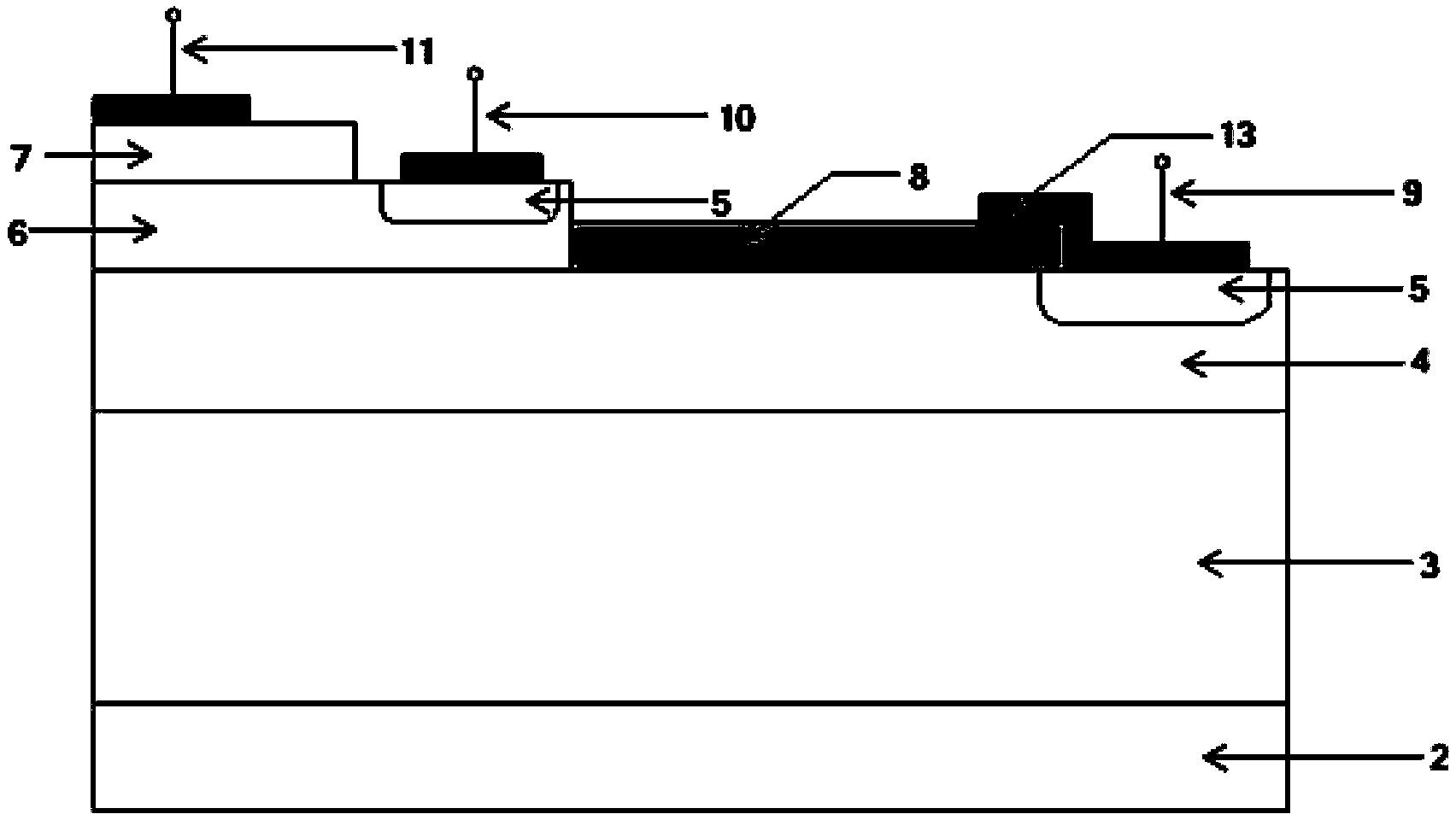
[0033] Another specific implementation of the lateral bipolar transistor with field plate structure described in the present invention is given below, see image 3 As shown, the lateral bipolar transistor with a collector field plate structure in this embodiment includes a substrate 2, a buffer zone 3, a collector region 4, a base region 6, and an emitter region 7 from bottom to top. The ohmic contact region 5 is formed by ion implantation at the upper boundary of the collector region 4 and the base region 6, and metal deposition is performed on the collector region 4, the base region 6, and the emitter region 7 respectively. Metal electrodes are formed in a manner, the emitter 11 is located on the emitter region 7, the collector 9 is located on the ohmic contact region 5 of the collector region 4, and the base 10 is located between the ohmic contact region 5 of the base region 6 Above, a collector field plate 13 is arranged on the collector region 4, an oxide layer 8 is arran...

Embodiment 3

[0036] Another specific implementation of the lateral bipolar transistor with field plate structure described in the present invention is given below, see Figure 4 As shown, the lateral bipolar transistor with an emitter field plate structure in this embodiment includes a substrate 2, a buffer zone 3, a collector region 4, a base region 6, and an emitter region 7 from bottom to top, respectively. The ohmic contact region 5 is formed by ion implantation at the upper boundary of the collector region 4 and the base region 6, and metal deposition is performed on the collector region 4, the base region 6, and the emitter region 7 respectively. Metal electrodes are formed in a manner, the emitter 11 is located on the emitter region 7, the collector 9 is located on the ohmic contact region 5 of the collector region 4, and the base 10 is located between the ohmic contact region 5 of the base region 6 An emitter field plate 14 is arranged on the emitter region 7, an oxide layer 8 is a...


PUM


Abstract

The invention relates to an LBJT (lateral bipolar transistor) containing a field plate structure. The LBJT comprises a substrate, a buffer region, a collector region, a base region and an emitter region which are arranged from bottom to top, wherein ohmic contact regions are formed on the upper edges of the collector region and the base region in an ion implantation manner; metal electrodes are respectively formed in the collector region, the base region and the emitter region in a metal deposition manner; an emitting electrode is positioned in the emitter region; a collector electrode is positioned in the ohmic contact region of the collector region; a base electrode is positioned in the ohmic contact region of the base region. The LBJT is characterized in that oxidation layers are arranged on the exteriors of the collector region, the base region and the emitter region; at least one of the base region, the collector region and the emitter region is provided with a field plate. According to the invention, the field plate structure is adopted to enhance the depletion of a drift region so as to reduce the peak electric field in the drift region; thus, a higher blocking voltage can be born under the condition of the same length of the drift region, and the voltage blocking grade of the device is remarkably increased.

Description

technical field [0001] The invention relates to a transistor, in particular to a lateral bipolar transistor with a field plate structure. Background technique [0002] The application of power electronics integration technology is becoming more and more extensive in today's society. However, due to the complexity of power electronic devices, there are huge obstacles to the wide application of power electronics integration technology. On the one hand, many fields need to use a large number of power electronic devices, and on the other hand, the applications of power electronic devices vary widely, which makes design, production and maintenance require a lot of manpower and material resources, causing huge obstacles to popularization and promotion. bottleneck to progress. [0003] At present, the international power electronics community generally believes that power electronics integration technology is the most promising way to solve the obstacles faced by the development o...

Claims


Application Information

Patent Timeline
Patent Type & Authority Applications(China)
IPC IPC(8): H01L29/735H01L29/40
CPCH01L29/735H01L29/402
Inventor 崔京京张作钦
Owner SUZHOU YINGNENG ELECTRONICS TECH
Why Eureka
Try Eureka