

Dielectric waveguide filter with defected ground loaded on magnetic coupling structure
A defected structure, dielectric waveguide technology, applied in waveguide-type devices, circuits, electrical components, etc., can solve the influence of high-order modes of waveguides that fail to meet design requirements, limited use of integrated dielectric waveguide filters, and high-end out-of-band suppression It is not a very high problem, and achieves the effect of good out-of-band suppression, compact structure, and compressed length.
- Summary
- Abstract
- Description
- Claims
- Application Information
AI Technical Summary
Problems solved by technology
Method used
Image

Examples
Embodiment Construction
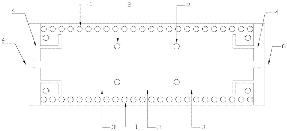
[0025] Such as image 3 , 4As shown, a magnetically coupled dielectric waveguide filter with a defect-loaded structure proposed by the present invention is to punch a row of metallized through holes 1 on both sides of the dielectric substrate, and the diameter of the metallized through holes 1 is less than one-fifth Waveguide wavelength, the interval between the holes is less than twice the diameter of the hole, the electromagnetic wave is limited to the upper and lower metal surfaces of the substrate and the area between the two rows of metal through holes to propagate, forming a dielectric waveguide transmission line. On the formed dielectric waveguide transmission line, two pairs of symmetrical metallized through-holes 2 are punched perpendicular to the horizontal center line, and the dielectric waveguide transmission line is divided into three parts, and these three parts are dielectric waveguide resonators 3, and the two A magnetic coupling structure is formed for the le...
PUM
 Abstract
Description
Claims
Application Information