Preparation method for thin-film sample for high-resolution transmission electron microscope
A transmission electron microscope, high-resolution technology, applied in the field of electron microscope thin film sample preparation, can solve the problem of inability to realize microstructure analysis, and achieve the effects of shortening ion thinning time, inhibiting damage, and shortening sample preparation cycle.
- Summary
- Abstract
- Description
- Claims
- Application Information
AI Technical Summary
Problems solved by technology
Method used
Image
Examples
preparation example Construction
[0011] The invention provides a method for preparing a high-resolution transmission electron microscope film sample of a special sample. The preparation process is as follows:
[0012] Cut a block sample from the sample containing the observed position. The size of the block sample is: length: 0.5-2.2mm, width: 0.5-1mm, thickness: 0.2-0.5mm; at the same time, place the observed position on the block Near the center of the surface of the shape sample composed of length and thickness;
[0013] Cut a piece of ingredients with the same size and material as the block sample to be observed;
[0014] The observed surface of the block sample is glued to the ingredients to form a glued sample;
[0015] Grind evenly the two surfaces in the thickness direction of the adhesive sample, and finally use 1000# sandpaper to grind to 20-30 μm to form an adhesive sheet;
[0016] Stick the opposite-adhesive sheet on the single-hole ring carrier;
[0017] Thin the single-hole annular carrier gr...
Embodiment 1
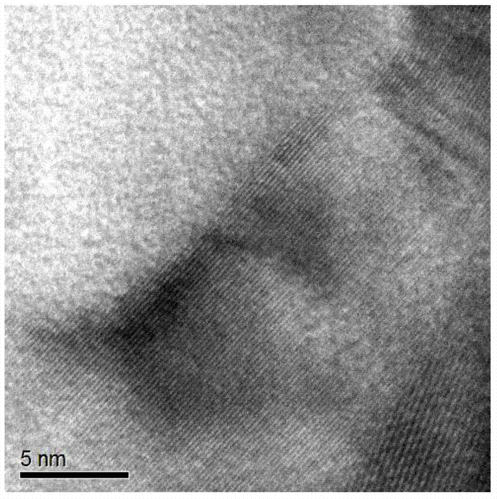
[0029] High-resolution electron microscopy thin film samples of the degenerated layer on the ground surface of the superalloy GH4169 plate were prepared. The sample preparation process is as follows: 1) Cut two block samples on the GH4169 plate. The size of the block sample is: length: 2.2mm, width: 1mm: thickness: 0.3mm, and the grinding surface On the surface of the sample composed of length and thickness; 2) Two pieces of block samples are glued to each other, and two of the facing surfaces are the grinding surfaces of the GH4169 plate; 3) Two blocks in the thickness direction of the bonding Grind the surface evenly, and finally grind it to 22.7 μm with 1000# sandpaper to form a bonding sheet; 4) Stick the bonding sheet to a single-hole ring carrier with an inner hole diameter of 1mm; 5) Stick the bonding sheet to a single hole The annular grid is placed on the ion thinner and thinned to perforation.
[0030] The ion thinning process parameters are: 1) The ion beam voltage...
Embodiment 2
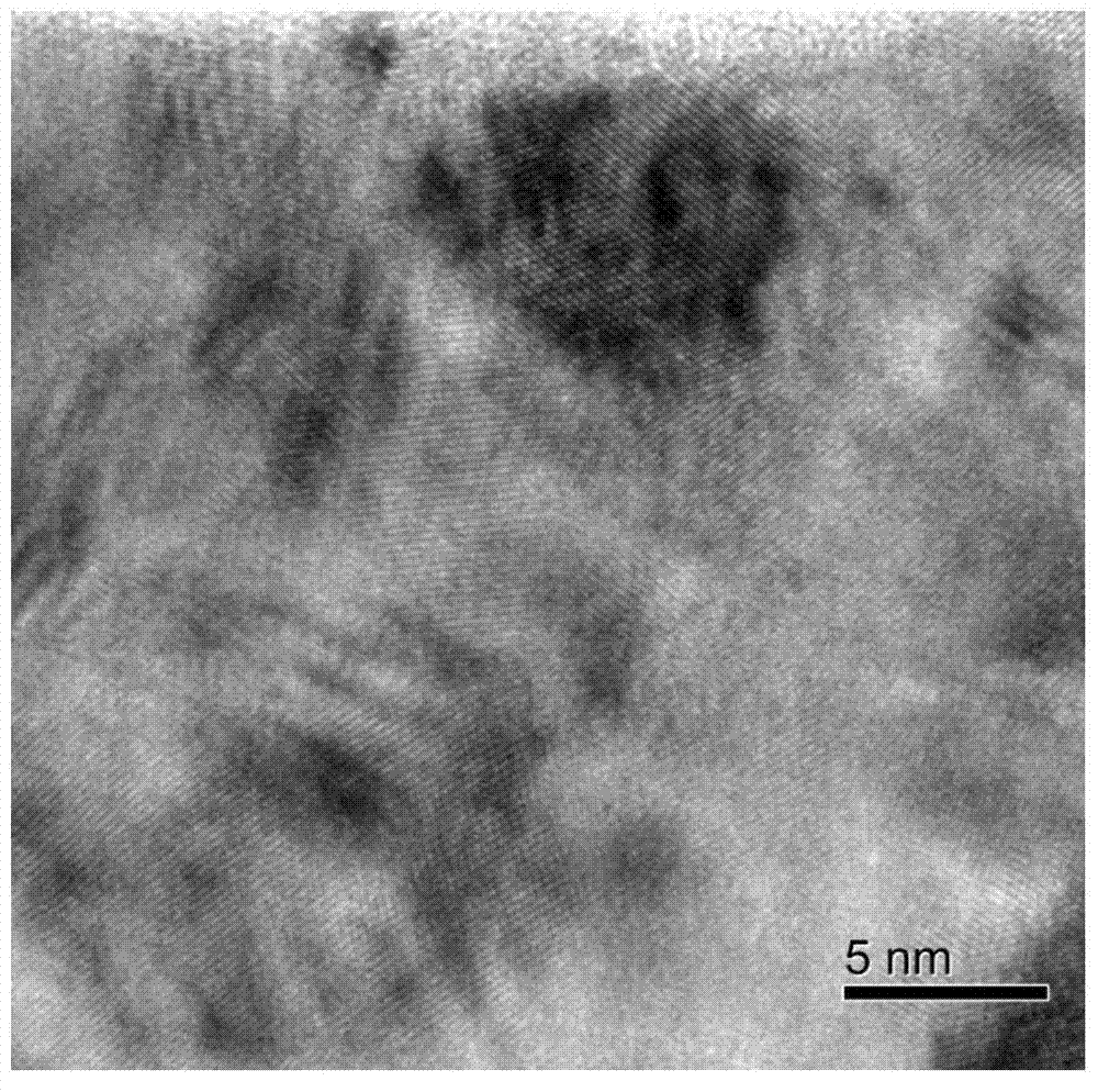
[0033] High-resolution electron microscopy thin film samples of the degenerated layer on the grinding surface of the ultra-high-strength steel M50NiL sheet were prepared. The sample preparation process is as follows: 1) Cut two block samples from the ultra-high strength steel M50NiL plate. The size of the block sample is: length: 2.2mm, width: 1mm: thickness: 0.3mm, and the surface Place on the surface of the block sample consisting of length and thickness; 2) Bond two block samples, and both of the bonding surfaces are grinding surfaces of M50NiL plates; 3) Make the thickness of the bonding sample The two surfaces in the same direction are evenly polished, and finally ground to 21.2 μm with 1000# sandpaper to form a counter-adhesive sheet; 4) Adhere the counter-adhesive sheet to a single-hole ring carrier with an inner hole diameter of 1mm; 5) Adhesive the counter-adhesive sheet The single-hole annular carrier grid of the sheet is thinned to perforation on the ion thinner.
...
PUM
| Property | Measurement | Unit |
|---|---|---|
| Size | aaaaa | aaaaa |
| Bore diameter | aaaaa | aaaaa |
| Outer diameter | aaaaa | aaaaa |
Abstract
Description
Claims
Application Information


