IGZO (Indium Gallium Zinc Oxide) transistor structure, manufacture method and display panel thereof

A manufacturing method and transistor technology, applied in semiconductor/solid-state device manufacturing, transistors, electric solid-state devices, etc., can solve problems such as damaging IGZO channels, ignoring IGZO channel protection, and affecting ohmic contact performance, so as to improve device characteristics , Improve the effect of ohmic contact

Active Publication Date: 2014-04-02
TCL CHINA STAR OPTOELECTRONICS TECH CO LTD
View PDF4 Cites 12 Cited by
  • Summary
  • Abstract
  • Description
  • Claims
  • Application Information

AI Technical Summary

Problems solved by technology

[0004] However, in the existing manufacturing methods, especially when the N-type doping of IGZO is performed by plasma treatment, the

Method used


Image

  • IGZO (Indium Gallium Zinc Oxide) transistor structure, manufacture method and display panel thereof
  • IGZO (Indium Gallium Zinc Oxide) transistor structure, manufacture method and display panel thereof
  • IGZO (Indium Gallium Zinc Oxide) transistor structure, manufacture method and display panel thereof

Examples


Embodiment 1

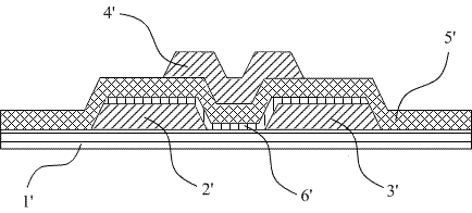
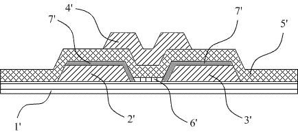
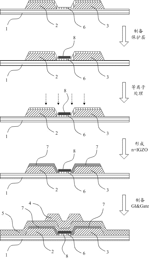
[0070] please refer again Figure 5 As shown, corresponding to Embodiment 1 of the present invention, Embodiment 3 of the present invention provides an IGZO transistor structure, including:

[0071] The source 2, the drain 3 and the IGZO 6 arranged on the substrate 1;

[0072] a protective layer 8 overlying the IGZO 6 channel;

[0073] n+IGZO region 7 formed by N-type doping in the contact region of source 2, drain 3 and IGZO 6;

[0074] a gate insulating layer 5 disposed over the protection layer 8 and the n+IGZO region 7; and

[0075] The gate 4 is provided on the gate insulating layer 5 .

[0076] Wherein, the protective layer 8 is silicon oxide.

[0077] In this embodiment, since the protective layer 8 is set above the IGZO 6 channel in the IGZO transistor structure, it can prevent the damage to the IGZO 6 channel in the plasma treatment process, and the PECVD film formation will not damage the IGZO 6 channel road. In addition, after the preparation of the protective...


PUM


Abstract

The invention provides an IGZO (Indium Gallium Zinc Oxide)transistor, a manufacture method and a display panel thereof, wherein the manufacture method of the IGZO transistor comprises the following steps: preparing a source/drain electrode pattern layer and an IGZO pattern layer on a substrate; preparing a protective layer on an IGZO channel; performing N-shaped mix on the region where source/drain electrodes are in contact with an IGZO via plasma treatments to form an n+IGZO region; preparing a gate insulation layer and a gate pattern layer. Via the IGZO transistor, the manufacture method and the display panel, the problem of damaging the IGZO channel in the process of performing the N-shaped mix on the IGZO via the plasma treatments can be solved, and the method is helpful to improve ohmic contact and increase element characteristics.

Description

technical field [0001] The invention relates to the field of image display, in particular to a method for manufacturing an indium gallium zinc oxide semiconductor IGZO transistor. Background technique [0002] Thin-film field-effect transistors (TFTs) based on oxide semiconductors are a hot topic in the future display field, and have been extensively researched and developed in recent years. Among them, the amorphous indium gallium zinc oxide (a-IGZO) film used as the active channel layer has a mobility as high as 80cm2 / Vs (the mobility of amorphous silicon a-Si is only 0.5~0.8cm2 / Vs), and can Compatible with a-Si large-scale mass production process. Therefore, the potential application of indium gallium zinc oxide semiconductor IGZO in next-generation liquid crystal displays (LCDs) and organic light-emitting diodes (OLEDs). [0003] When the metal and IGZO are in contact, the semiconductor energy band bends at the interface to form a potential barrier. The presence of a ...

Claims


Application Information

Patent Timeline
IPC IPC(8): H01L29/786H01L21/77H01L27/12
CPCH01L29/7869H01L29/66969H01L29/1083H01L29/78696
Inventor 石龙强曾志远
Owner TCL CHINA STAR OPTOELECTRONICS TECH CO LTD
Why Eureka
Try Eureka