
Light emitting diode and manufacturing method thereof

A technology for light-emitting diodes and a manufacturing method, which is applied to electrical components, circuits, semiconductor devices, etc., can solve the problems of photons not escaping, chip light loss, etc., and achieve the effects of reducing total reflection absorption, improving light output efficiency, and improving brightness.

Active Publication Date: 2014-04-09
EPILIGHT TECH
View PDF4 Cites 4 Cited by
  • Summary
  • Abstract
  • Description
  • Claims
  • Application Information

AI Technical Summary

Problems solved by technology

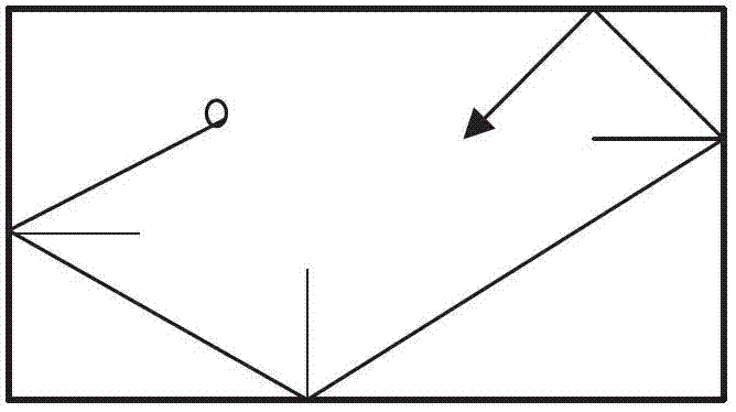
figure 2 This is the light output effect diagram of a traditional quadrilateral chip. For a traditional light-emitting diode, when the incident angle of light is greater than 23.5° and less than 66.5°, the light of the chip will only be reflected back and forth inside the chip, and photons cannot escape from the chip. external, resulting in light loss from the chip

Method used


Image

  • Light emitting diode and manufacturing method thereof
  • Light emitting diode and manufacturing method thereof
  • Light emitting diode and manufacturing method thereof

Examples


Embodiment Construction

[0034] The implementation of the present invention will be illustrated by specific specific examples below, and those skilled in the art can easily understand other advantages and effects of the present invention from the contents disclosed in this specification. The present invention can also be implemented or applied through other different specific implementation modes, and various modifications or changes can be made to the details in this specification based on different viewpoints and applications without departing from the spirit of the present invention.

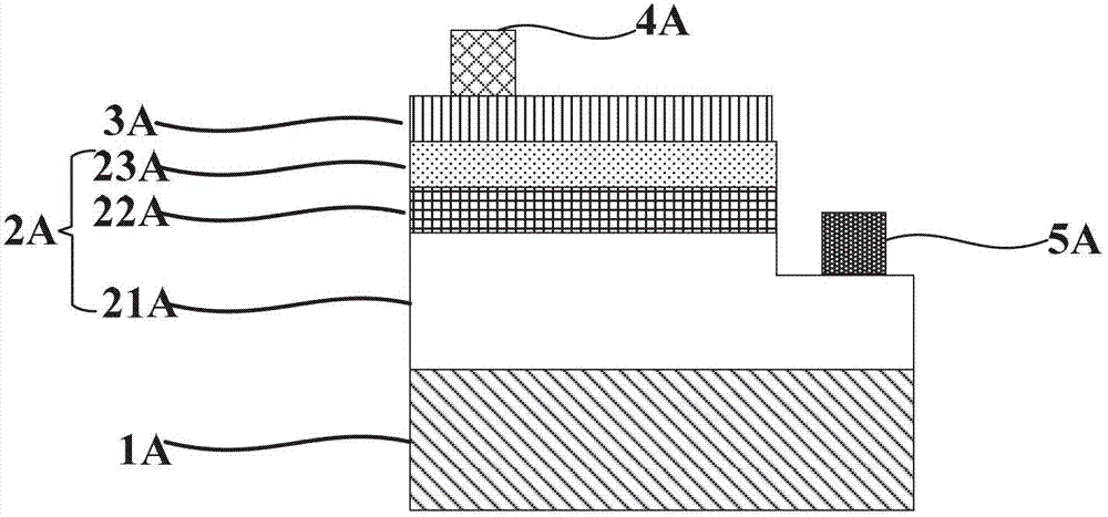
[0035] see Figure 3~5 . It should be noted that the diagrams provided in this embodiment are only schematically illustrating the basic idea of ​​the present invention, and only the components related to the present invention are shown in the diagrams rather than the number, shape and shape of the components in actual implementation. Dimensional drawing, the type, quantity and proportion of each component can be cha...


PUM


Abstract

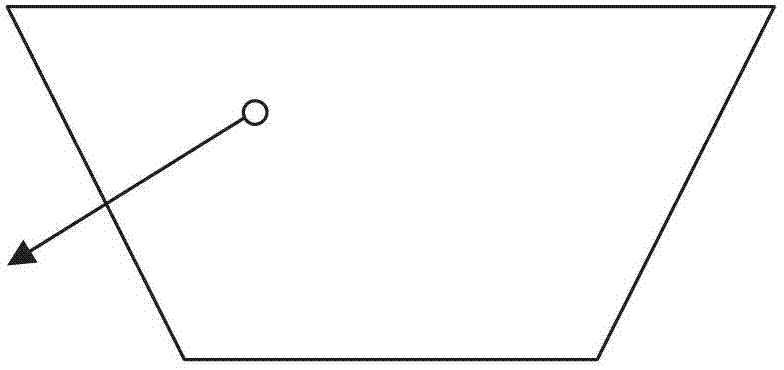
The invention provides a light emitting diode and a manufacturing method thereof. The method comprises the following steps: preparing a selective growth layer on a surface of a substrate first; then, selectively growing a light emitting structure layer in an epitaxial mode in a non-selective growth layer region of the surface of the substrate, wherein the light emitting structure layer is of an inverted trapezoidal structure and at least includes an N-type semiconductor layer, a quantum well layer and a P-type semiconductor layer; etching to an N electrode region with the use of the photo-etching technology, the ICP technology or the RIE technology; making a transparent conductive layer; making a P electrode and an N electrode; preparing a first reflective mirror layer on the transparent conductive layer and preparing a second reflective mirror layer on the other surface of the substrate; and finally, carrying out splintering to complete preparation of the independent light emitting diode. According to the light emitting diode prepared by using the epitaxial selective growth technology, total reflection absorption of a chip to light can be reduced, light can be emitted out from the inside of the light emitting diode, the light extraction efficiency of light on the side wall of the chip is improved, and the excitation efficiency of fluorescent powder is improved and the brightness of the chip is improved due to the adoption of two-way reflective mirrors.

Description

technical field [0001] The invention relates to a light-emitting diode and a manufacturing method thereof, in particular to a light-emitting diode with an inverted trapezoidal structure and a manufacturing method thereof. Background technique [0002] Light-emitting diode (LED) has the characteristics of green environmental protection, long life, high efficiency and energy saving, anti-harsh environment, simple structure, small size, light weight, fast response, low working voltage and good safety, so it is known as the successor to incandescent lamps, The fourth generation of lighting power supply after fluorescent lamps and energy-saving lamps. In the mid-1990s, through unremitting efforts, Japan’s Nichia Chemical Company broke through the key technology of manufacturing blue light-emitting diodes, and developed the technology of covering blue LEDs with phosphors to produce white light sources. However, there are still many problems to be solved in semiconductor lighting,...

Claims


Application Information

Patent Timeline
Patent Type & Authority Applications(China)
IPC IPC(8): H01L33/10H01L33/20H01L33/00
CPCH01L33/46H01L2933/0025H01L33/20H01L33/0095
Inventor 张楠郝茂盛
Owner EPILIGHT TECH
Learn More