Organic light emitting diode and electronic equipment
A technology of light-emitting diodes and light-emitting sub-layers, which is applied in the direction of organic light-emitting devices, organic light-emitting device structures, organic semiconductor devices, etc., can solve problems such as high voltage, high power consumption, and increased process complexity with the number of layers, so as to reduce the working voltage , The effect of reducing the number of layers and reducing power consumption
- Summary
- Abstract
- Description
- Claims
- Application Information
AI Technical Summary
Problems solved by technology
Method used
Image

Examples
preparation example Construction
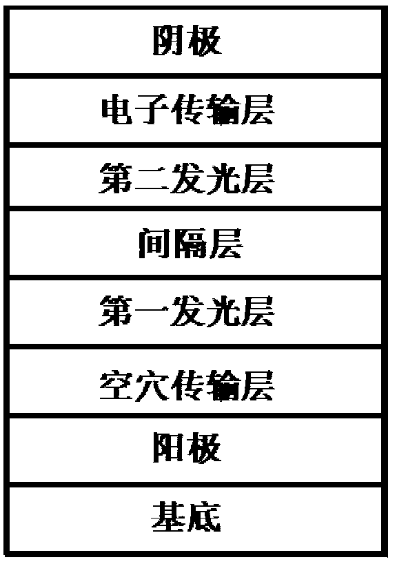
[0073] The preparation of the above light-emitting layer is described below.
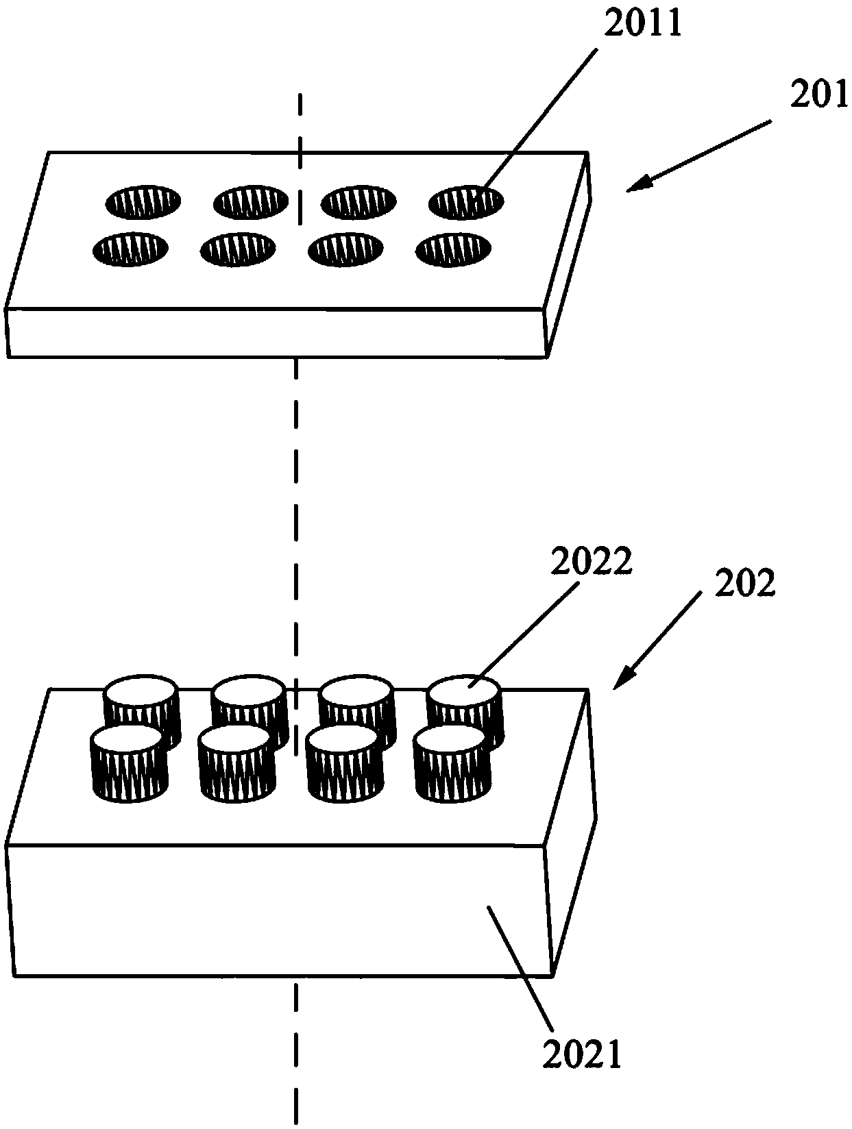
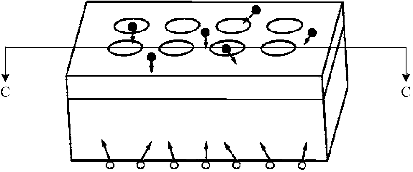
[0074] Such as figure 2 As shown, if the second luminescent sublayer is closer to the glass substrate, at this time, for the preparation of the luminescent layer, the following steps are included:
[0075] first forming a second luminescent material layer;
[0076] Then through a MASK process can be obtained as figure 2 the protrusion shown;
[0077] Finally, the first luminescent material layer is formed, and since part of the area is blocked by the protruding part, a hollow structure is naturally formed.
[0078] If the first luminescent sublayer is closer to the glass substrate, the preparation of the luminescent layer includes the following steps:
[0079] first forming a first luminescent material layer;
[0080] Then through a MASK process or printing process, you can get such figure 2 The first light-emitting layer with a hollow structure shown;
[0081] Finally, the second luminesc...
PUM
 Abstract
Description
Claims
Application Information
 - R&D
- Intellectual Property
- Life Sciences
- Materials
- Tech Scout
- Unparalleled Data Quality
- Higher Quality Content
- 60% Fewer Hallucinations
Browse by: Latest US Patents, China's latest patents, Technical Efficacy Thesaurus, Application Domain, Technology Topic, Popular Technical Reports.
© 2025 PatSnap. All rights reserved.Legal|Privacy policy|Modern Slavery Act Transparency Statement|Sitemap|About US| Contact US: help@patsnap.com