Forming method of packaging structure

A technology of packaging structure and plastic packaging layer, which is applied in the manufacture of electrical components, electric solid-state devices, semiconductor/solid-state devices, etc.

Active Publication Date: 2014-04-16
NANTONG FUJITSU MICROELECTRONICS
View PDF9 Cites 8 Cited by
  • Summary
  • Abstract
  • Description
  • Claims
  • Application Information

AI Technical Summary

Problems solved by technology

[0004] Existing lead frame packages can only be packaged for a single semiconductor chip and lead frame, and the packaging efficiency is low

Method used


Image

  • Forming method of packaging structure
  • Forming method of packaging structure
  • Forming method of packaging structure

Examples


Embodiment Construction

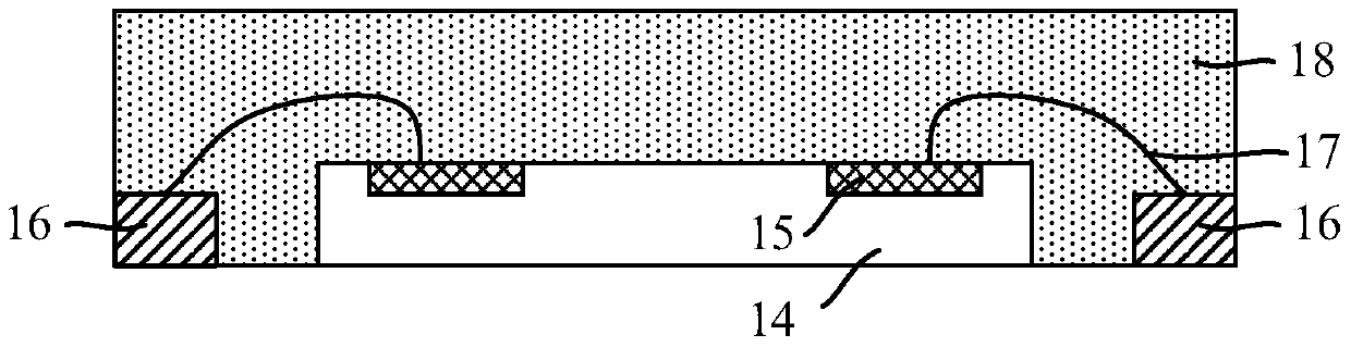
[0024] When encapsulating existing leadframes, please refer to the figure 1 First, the wafer needs to be cut to form semiconductor chips 14 one by one, and then metal wires 17 are formed through a wire bonding process. The metal wires 17 connect the pads 15 on the semiconductor chips 14 with the surrounding pins 16, and finally pass The plastic encapsulation material 18 encapsulates the semiconductor chip 14 and the pins 16. The existing packaging process can only realize the packaging of a single semiconductor chip and pins, and the encapsulation efficiency is low. In addition, the pins 16 are arranged around the semiconductor chip 14, and the pads 15 on the semiconductor chip 14 need to be electrically connected to the surrounding pins 16 through metal wires 17, so that the volume occupied by the entire packaging structure is relatively large. , which is not conducive to the improvement of the integration degree of the packaging structure.

[0025]For this reason, the prese...


PUM


Abstract

Provided is a forming method of a packaging structure. The forming method comprises the steps that a pre-packaging face plate is provided, wherein the pre-packaging face plate comprises a first plastic-packaging layer, a plurality of integration units arrayed in a matrix mode are arranged in the first plastic-packaging layer, at least one semiconductor chip is arranged in each integration unit, a plurality of welding discs are arranged on the surfaces of the semiconductor chips, and the welding discs are provided with metal protruding blocks; a lead frame is provided, wherein the lead frame comprises a first surface and a second surface opposite to the first surface, the lead frame is provided with a plurality of bearing units arrayed in a matrix mode and middle ribs used for fixing the bearing units, each bearing unit is provided with a plurality of pins, openings are formed between adjacent pins, the pre-packaging face plate is inversely arranged on the first surface of the lead frame, so that the integration units correspond to the bearing units, and the metal protruding blocks and the first surfaces of the pins are welded. The occupied area of the packaging structure is small, and the integration level of the packaging structure is improved.

Description

technical field [0001] The invention relates to the field of semiconductor packaging, in particular to a method for forming a packaging structure. Background technique [0002] With the development of electronic products such as mobile phones and notebook computers towards miniaturization, portable, ultra-thin, multimedia and low-cost to meet the needs of the public, high-density, high-performance, high-reliability and low-cost packaging forms and their Assembly technology has been rapidly developed. Compared with expensive packaging forms such as BGA (Ball Grid Array), new packaging technologies that have developed rapidly in recent years, such as Quad Flat No-lead Package (QFN) due to its good thermal performance and electrical The advantages of performance, small size, low cost and high productivity have triggered a new revolution in the field of microelectronic packaging technology. [0003] figure 1 It is a structural schematic diagram of an existing QFN packaging st...

Claims


Application Information

Patent Timeline
Patent Type & Authority Applications(China)
IPC IPC(8): H01L21/50
CPCH01L21/50H01L24/81H01L2224/81H01L24/96H01L24/97H01L2224/12105H01L2224/16245H01L2224/48091H01L2224/48247H01L2924/181H01L2924/18165H01L2924/3511H01L2924/00014H01L2924/00012
Inventor 陶玉娟
Owner NANTONG FUJITSU MICROELECTRONICS
Why Eureka
Try Eureka