
Polycrystalline silicon ingot casting molten material and impurity removing process

A technology of polysilicon and melting materials, which is applied in the direction of polycrystalline material growth, crystal growth, single crystal growth, etc., can solve problems affecting the yield of slicing, high carbon content of silicon ingots, and low efficiency of cells, so as to eliminate polysilicon ingots Quality reduction, low input cost, easy to master effect

Inactive Publication Date: 2014-04-23
XIAN HUAJING ELECTRONICS TECH
View PDF4 Cites 13 Cited by
  • Summary
  • Abstract
  • Description
  • Claims
  • Application Information

AI Technical Summary

Problems solved by technology

However, in the actual melting process, the gas in the ingot furnace cannot immediately discharge the heat field through the gas outlet, but will circulate in the combined structure composed of the crucible, guard plate, cover plate, etc., and enter the surface of the silicon melt, making it The carbon element is adsorbed and dissolved into the silicon melt, correspondingly making SiC, Si 3 N 4 Other impurities enter the silicon ingot, resulting in high carbon content in the grown silicon ingot, resulting in ingot defects, affecting the yield of slicing, and ultimately leading to low efficiency of the cell

Method used

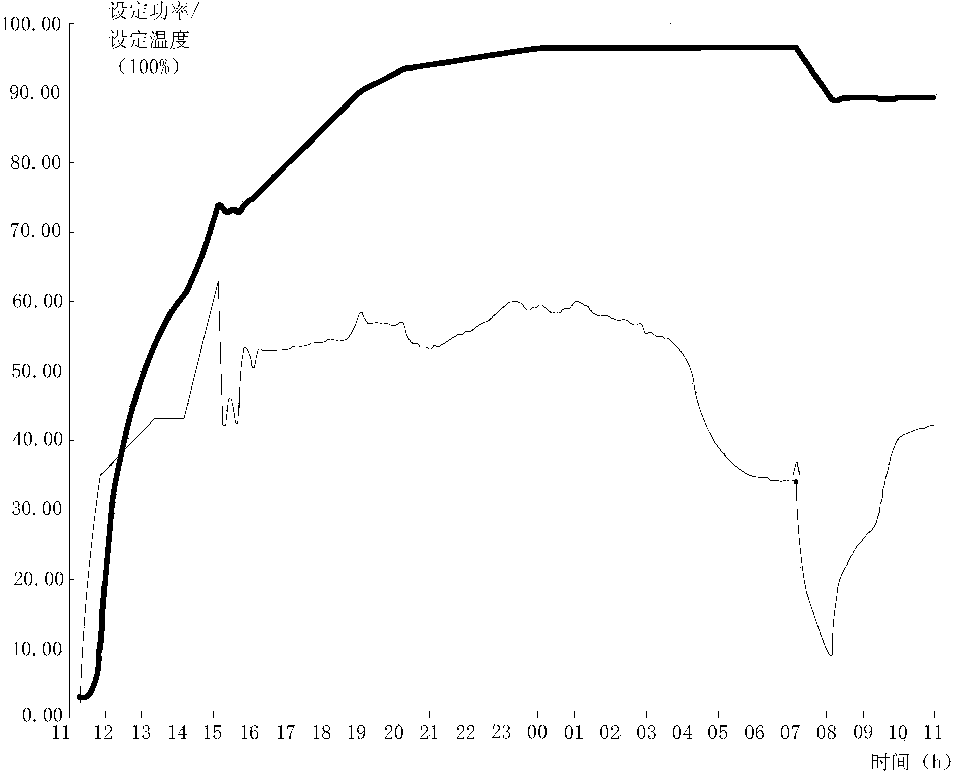

Image

  • Polycrystalline silicon ingot casting molten material and impurity removing process
  • Polycrystalline silicon ingot casting molten material and impurity removing process

Examples


Embodiment 1

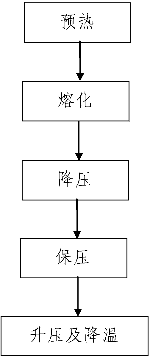
[0040] Such as figure 1 The shown polysilicon ingot molten material and impurity removal process includes the following steps:

[0041] Step 1. Preheating: Preheat the silicon material contained in the crucible with an ingot furnace, and gradually increase the heating temperature of the ingot furnace to T1; the preheating time is 7h, where T1=1175°C.

[0042] In this embodiment, the ingot furnace is a G5 ingot furnace. In addition, the ingot furnace is specifically a G5 ingot furnace produced by Zhejiang Jingsheng Electromechanical Co., Ltd. The crucible is a quartz crucible and it is a G5 crucible, and the produced polysilicon ingot is a G5 ingot.

[0043] In actual use, the charging amount of the quartz crucible is about 600 kg.

[0044] In this embodiment, the charging amount of the quartz crucible is 560 kg. In actual use, the charging amount of the quartz crucible can be adjusted according to specific needs.

[0045] In this embodiment, during the preheating process in step 1, t...

Embodiment 2

[0084] In this embodiment, the difference from embodiment 1 is: the preheating time in step 1 is 6h and T1=1185°C, P1=80kW; in step 2, T5=1560°C, t=18min, Q1=650mbar; step 1. The medium holding time is 0.4h; from step 2 to step 5, T2=1210℃, and the heating time is 0.4h; in step 6 T3=1460℃ and the heating time is 3.5h; in step 7, T4=1510℃ and The heating time is 3.5h; in the 8th step, T5=1560℃ and the heating time is 3.5h; the 9th step is 3.5h; the 10th step is 4h.

[0085] In this embodiment, the process of heating and pressurizing in steps 2 to 5 is as follows:

[0086] The second step, the first step is to increase: the heating temperature of the ingot furnace is increased from 1185°C to 1190°C, and the heating time is 5 min.

[0087] Step 3 and Step 2: Increase the heating temperature of the ingot furnace from 1190°C to 1195°C, and the heating time is 5 minutes.

[0088] Step 4 and Step 3: Raise the heating temperature of the ingot furnace from 1195°C to 1205°C, and the heating ti...

Embodiment 3

[0095] In this embodiment, the difference from embodiment 1 is: the preheating time in step one is 10h and T1=1165°C, P1=70kW; in step two, T5=1540°C, t=22min, Q1=550mbar; step 1. The medium holding time is 0.6h; from step 2 to step 5, T2=1190℃ and the heating time is 0.6h; in step 6 T3=1440℃ and the heating time is 4.5h; in step 7 T4=1490℃ and The heating time is 4.5h; in the 8th step, T5=1540℃ and the heating time is 4.5h; the 9th step is 4.5h; the 10th step is 8h.

[0096] In this embodiment, the process of heating and pressurizing in steps 2 to 5 is as follows:

[0097] The second step, the first step is to increase: increase the heating temperature of the ingot furnace from 1165°C to 1172°C, and the heating time is 9 minutes.

[0098] Step 3 and Step 2: Increase the heating temperature of the ingot furnace from 1172°C to 1178°C, and the heating time is 8 minutes.

[0099] Step 4 and Step 3: Increase the heating temperature of the ingot furnace from 1178°C to 1183°C, and the heat...


PUM


Abstract

The invention discloses a polycrystalline silicon ingot casting molten material and an impurity removing process. The process comprises the following steps: 1, preheating: adopting an ingot furnace to preheat a silicon material filled in a crucible, and gradually raising the heating temperature of the ingot furnace to T1; the preheating time is 6-10h, and T1=1165-1185 DEG C; 2, melting: the melting temperature is T1-T5; T5=1540-1560 DEG C; in the melting process, filling insert gases into the ingot furnace, and keeping air pressure in the furnace in Q1, and Q1=550-650mbar; 3, removing impurities: the process is as follows: the 11th step, reducing pressure: the air pressure of the ingot furnace is reduced from Q1 to Q2, and the pressure reducing time is 8-12min, and Q2=350-450mbar; the 12th step, maintaining pressure; the 13th step, boosting pressure and lowering temperature. The process has the advantages of simple steps, reasonable design, convenience in realization, easiness in grasp and good using effect, can discharge gas containing carbon in the furnace in time, and increases the polycrystalline silicon ingot casting quality.

Description

Technical field [0001] The invention belongs to the technical field of polycrystalline silicon ingots, and particularly relates to a polycrystalline silicon ingot melting material and a process for removing impurities. Background technique [0002] Photovoltaic power generation is one of the most important clean energy sources and has great development potential. The key factors restricting the development of the photovoltaic industry are the low photoelectric conversion efficiency on the one hand, and the high cost on the other. Photovoltaic silicon wafers are the basic material for the production of solar cells and modules. The purity of polysilicon used to produce photovoltaic silicon wafers must be above 6N (that is, the total content of non-silicon impurities is below 1ppm), otherwise the performance of photovoltaic cells will be greatly negatively affected. influences. In recent years, polycrystalline silicon wafer production technology has made significant progress. Poly...

Claims


Application Information

Patent Timeline
Patent Type & Authority Applications(China)
IPC IPC(8): C30B11/00C30B28/06C30B29/06
Inventor 周建华
Owner XIAN HUAJING ELECTRONICS TECH
Learn More