

Flexible circuit substrate double-sided light-emitting LED array light source
A flexible circuit substrate, LED array technology, applied in the direction of circuits, electrical components, electric solid devices, etc., can solve the problems of poor light extraction efficiency and low light source utilization rate, and achieve the goal of improving conversion efficiency, high degree of automation, and improved light extraction efficiency Effect
- Summary
- Abstract
- Description
- Claims
- Application Information
AI Technical Summary
Problems solved by technology
Method used
Image


Examples
Embodiment Construction
[0028] The present invention will be further described below in conjunction with the accompanying drawings.
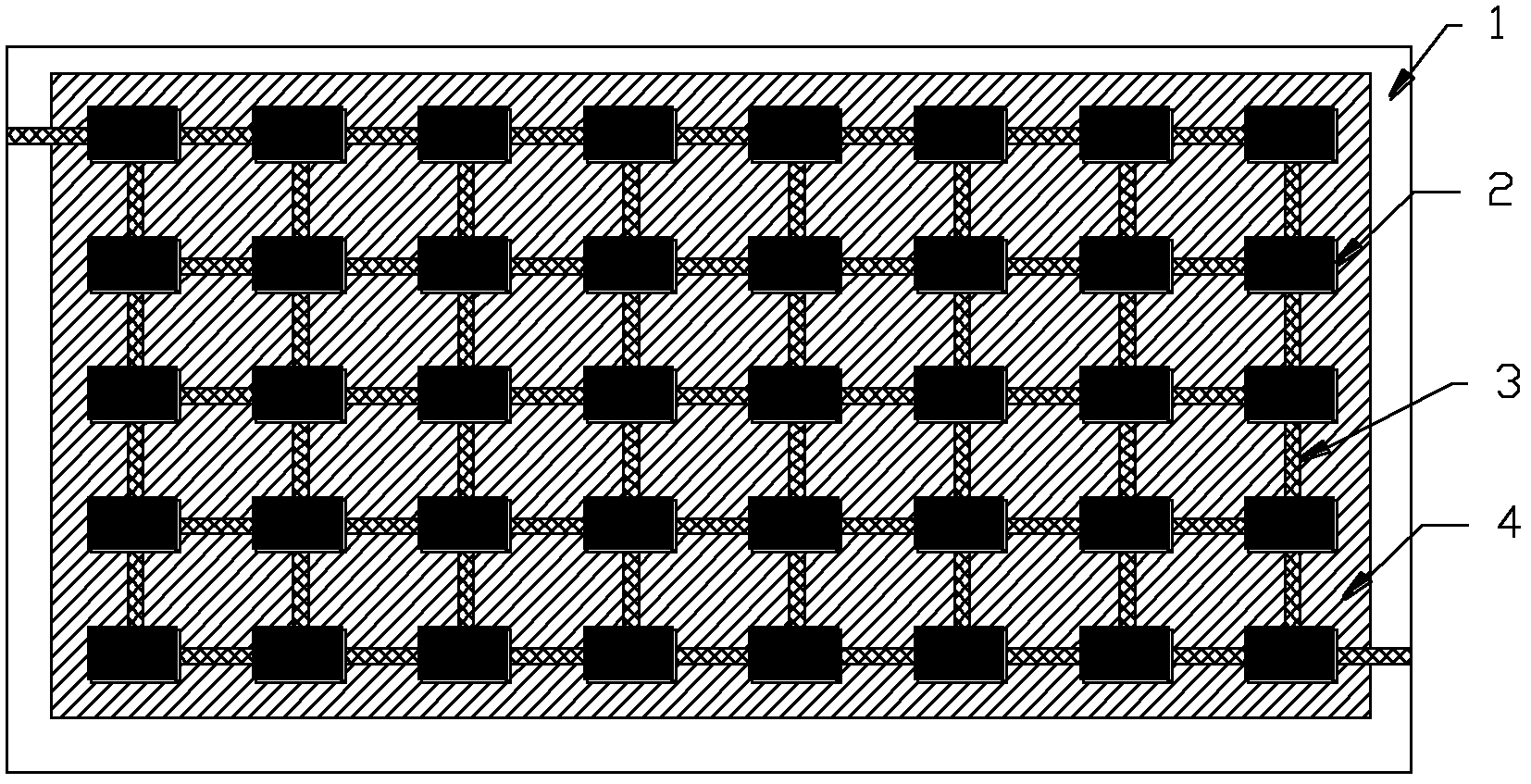
[0029] Such as Figure 1-2 As shown, a flexible circuit substrate double-sided LED array light source, including a flexible planar transparent circuit substrate 1, several LED chips 2, conductive patterns 3 and fluorescent films 4, on one side of the flexible planar transparent circuit substrate 1 A conductive pattern 3 is provided, and a bonding area is reserved on the conductive pattern 3. The LED chip 2 is directly mounted on the bonding area, and is connected to each other through the conductive pattern 3. One or two fluorescent films are arranged on the LED array. 4 Encapsulating the LED chip 2 as a whole. The light emitted by the LED chip 2 through the PN junction is converted into visible light by the fluorescent film 4 and emitted to both sides.
[0030] The flexible planar transparent circuit substrate 1 has a temperature resistance of more than 250 degrees ...
PUM
| Property | Measurement | Unit |
|---|---|---|
| Heat resistant | aaaaa | aaaaa |
| Thickness | aaaaa | aaaaa |
| Tensile strength | aaaaa | aaaaa |
Abstract
Description
Claims
Application Information