Three-dimensional integrated multi-layer stacked micro-shielded mems filter bank
A multi-layer stacking, three-dimensional integration technology, applied in waveguide-type devices, coupling of optical waveguides, components of TV systems, etc., to reduce the area, reduce microwave leakage, and facilitate integration.
- Summary
- Abstract
- Description
- Claims
- Application Information
AI Technical Summary
Problems solved by technology
Method used
Image
Examples
Embodiment
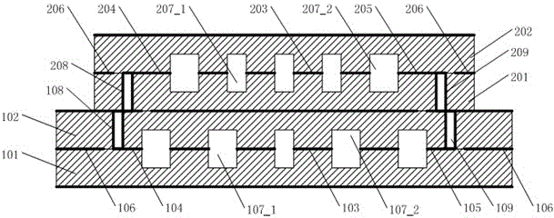
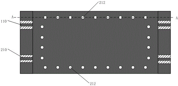
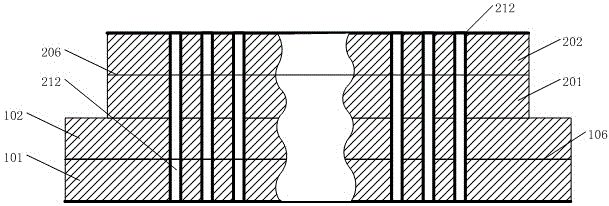
[0015] control figure 1 , 2 , 3, 4, three-dimensionally integrated multi-layer stack structure micro-shielding MEMS filter group, its structure includes A filter, B filter; described A filter includes A substrate 101 and B substrate 102, wherein in A Metal is deposited on the upper surface of the substrate 101 to form the A microwave coupling line resonator 103 , the A signal input transmission line 104 , the A signal output transmission line 105 and the A ground metal surface 106 .
[0016] The upper surface of the A substrate 101 and the lower surface of the B substrate 102 are aligned, and an A filter is formed by using a MEMS alignment bonding process.
[0017] Described B filter, its structure comprises C substrate 201 and D substrate 202, deposits metal on C substrate 201 upper surface to form B microwave coupled line resonator 203, B signal lead-in transmission line 204, B signal lead-out transmission line 205 and B ground metal plane 206 .
[0018] The upper surface...
PUM
 Abstract
Description
Claims
Application Information


