Storage capacitor, pixel unit and method for manufacturing storage capacitor

A technology for storing capacitors and pixel units, which is applied in the fields of electrical components, semiconductor/solid-state device manufacturing, circuits, etc., and can solve problems such as unstable display characteristics of the display panel, affecting the display characteristics of the display panel, and reducing the aperture ratio of the liquid crystal panel, so as to avoid Effects of releasing electrons, maintaining display characteristics, and reducing gaps

Inactive Publication Date: 2014-05-14
TCL CHINA STAR OPTOELECTRONICS TECH CO LTD
View PDF4 Cites 2 Cited by
  • Summary
  • Abstract
  • Description
  • Claims
  • Application Information

AI Technical Summary

Problems solved by technology

Among them, since the second metal layer electrically connected to the thin film transistor is accompanied by a semiconductor layer, the storage capacitor of the MIM structure will change its capacitance value when the positive and negative cycles are reversed, and the unstable storage capacitor will make the display characteristics of the display panel unstable. Stablize
In addition, since the semiconductor layer is wider than the second metal layer electrically connected to the thin film transistor, that is, the semiconductor layer will leak part of the second metal layer, which may release electrons, which will also affect the display characteristics of the display panel.
However, the gap between the storage capacitors of the MII architecture is relatively large. Since the capacitance is inversely proportional to the distance, if you want to obtain a larger storage capacitor value, you need to increase the area of ​​the storage capacitor, which will reduce the aperture ratio of the LCD panel.

Method used


Image

  • Storage capacitor, pixel unit and method for manufacturing storage capacitor
  • Storage capacitor, pixel unit and method for manufacturing storage capacitor
  • Storage capacitor, pixel unit and method for manufacturing storage capacitor

Examples


Embodiment 1

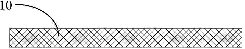
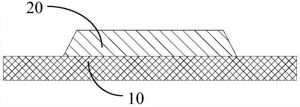
[0021] see Figure 1 to Figure 6 , a method for manufacturing a storage capacitor provided in the first embodiment of the present invention, comprising the following steps:

[0022] For a first step, see figure 1 , providing a substrate 10 made of glass or plastic. In this embodiment, the substrate 10 is made of glass.

[0023] In the second step, see figure 2 , forming a first metal layer on the substrate 10 , and patterning the first metal layer to form a first electrode 20 . Wherein, the first metal layer is a molybdenum layer, an aluminum layer, a titanium layer or a copper layer, or a stack of any two layers, and the first metal layer is formed on the substrate 10 by a sputtering process, and patterned The first metal layer is used to form the first electrode 20 using a photomask process.

[0024] Wherein, the photomask manufacturing process includes steps such as exposure, development, and etching. Specifically, firstly, a layer of photo-resist (photo-resistance) ...

Embodiment 2

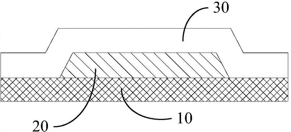
[0030] see Image 6 The storage capacitor 100 provided by the second embodiment of the present invention includes a substrate 10, a first electrode 20 formed on the substrate 10 and formed of a first metal layer, a first electrode 20 formed on the substrate 10 and the first electrode 20 An insulating layer 30, a semiconductor layer 40 formed on the first insulating layer 30, a second metal layer 50 formed on the semiconductor layer 40, formed on the first insulating layer 30, the semiconductor layer 40 and the second The second insulating layer 60 on the metal layer 50 and the pixel electrode 70 formed on the second insulating layer 60 and the second metal layer 50 as a second electrode.

[0031]The base 10 is made of glass or plastic. In this embodiment, the substrate 10 is made of glass. The first electrode 20 is a molybdenum layer, an aluminum layer, a titanium layer or a copper layer, or a stack of any two layers. The first insulating layer 30 is generally a SiNx layer....

Embodiment 3

[0034] See Figure 7 The pixel unit 200 provided by the third embodiment of the present invention is jointly defined by two adjacent scan lines 202 and two adjacent data lines 204 . The pixel unit 200 includes a thin film transistor 206 and a storage capacitor 100 as in the first embodiment. Wherein, the gate of the TFT 206 is electrically connected to the scan line 202 , the source is electrically connected to the data line 204 , and the drain is electrically connected to the pixel electrode 70 in the storage capacitor 100 . The scan line 202 provides a scan voltage to the thin film transistor 206 to turn on the thin film transistor 206 . The data line 204 provides the data voltage for the TFT 206, so that the pixel electrode 70 displays a gray scale corresponding to the data voltage, and the storage capacitor 100 stores the display voltage of the pixel electrode 70 during the off period of the TFT 206, that is, in Before the data is updated, the voltage of the pixel electr...


PUM


Abstract

The embodiment of the invention discloses a storage capacitor which comprises a substrate, a first electrode located on the substrate and formed by a first metal layer, a first insulating layer formed on the substrate and the first electrode, a semiconductor layer formed on the first insulating layer, a second metal layer formed on the semiconductor layer, a second insulating layer formed on the first insulating layer, the semiconductor layer and the second metal layer and a pixel electrode formed on the second insulating layer and the second metal layer and serving as a second electrode. A contact window is formed in the second insulating layer so that the second metal layer can be exposed. The pixel electrode is electrically connected with the exposed second metal layer through the contact window. In addition, the embodiment of the invention further discloses a pixel unit with the storage capacitor and a method for manufacturing the storage capacitor.

Description

technical field [0001] The present invention relates to the field of semiconductor manufacturing, in particular to a storage capacitor, a pixel unit with the storage capacitor and a manufacturing method of the storage capacitor. Background technique [0002] Thin Film Transistor Array (TFT Array) is an indispensable and important display component of Liquid Crystal Display (LCD). The TFT Array is mainly composed of multiple pixel units (pixel unit), multiple scan lines ( scan line) and multiple data lines (data line). These pixel units are electrically connected to the scan line and the data line, and each pixel unit has a thin film transistor, a liquid crystal capacitor (CLC) and a storage capacitor (storage capacitor, CS). Among them, the thin film transistor charges the liquid crystal capacitor to drive the liquid crystal molecules in the liquid crystal layer, so that the liquid crystal display displays images. At the same time, the thin film transistor charges the stora...

Claims


Application Information

Patent Timeline
Patent Type & Authority Applications(China)
IPC IPC(8): G02F1/136G02F1/1362G02F1/1368G02F1/1343H01L23/522H01L21/02
CPCG02F2201/40G02F2202/10G02F1/136213G02F1/133345H01L27/124H01L27/1255G02F1/133302G02F1/134309G02F1/13439G02F1/136286G02F1/1368G02F2201/123
Inventor 姚晓慧许哲豪
Owner TCL CHINA STAR OPTOELECTRONICS TECH CO LTD
Why Eureka
Try Eureka