In-situ morphology and optical performance monitoring evaporation source and vacuum deposition equipment

A technology of optical performance and evaporation source, applied in vacuum evaporation plating, ion implantation plating, metal material coating process, etc., can solve the problems of material performance degradation, failure, and electrons cannot reach the surface of the sample, etc.

Active Publication Date: 2014-05-21
SUZHOU UNIV
View PDF7 Cites 6 Cited by
  • Summary
  • Abstract
  • Description
  • Claims
  • Application Information

AI Technical Summary

Problems solved by technology

[0005] Electron diffraction technique is a commonly used technique for observing crystal growth process in situ. It is based on the diffraction of electrons of a single energy on the crystal surface to deduce the crystal surface structure, and is widely used in molecular beam epitaxy and organic molecules in single crystals. Surface self-organization; the disadvantage is that the substrate used must be conductive, or electrons cannot reach the sample surface due to charging
In addition, the high-energy electrons used may cause damage to materials, especially organic materials, resulting in material performance degradation or even failure
This technique can only obtain surface structure information, and other important information such as morphology and optical properties cannot be obtained; more importantly, this technique can only be applied to crystal materials
The further development of electron diffraction microscopy partially solves the shortcomings of electron diffraction technology, which can observe the morphology and obtain the contrast of different amorphous materials; however, the required conductive substrate and the destructiveness to the material still limit its further development. Generalize to all materials
Therefore, the existing vacuum deposition equipment still lacks components for direct observation of the surface of the deposited material, and cannot monitor the in-situ morphology and optical properties during crystal growth.

Method used


Image

  • In-situ morphology and optical performance monitoring evaporation source and vacuum deposition equipment
  • In-situ morphology and optical performance monitoring evaporation source and vacuum deposition equipment
  • In-situ morphology and optical performance monitoring evaporation source and vacuum deposition equipment

Examples


Embodiment 1

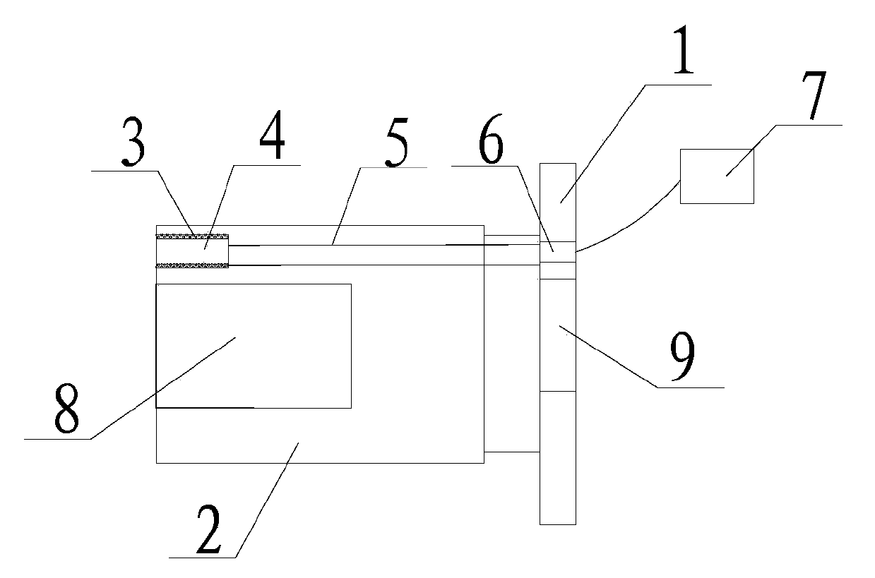
[0027] Such as image 3 The shown in-situ topography and optical performance monitoring evaporation source also includes a connected optical component 10 and an imaging component 11 in addition to the above-mentioned components. The optical assembly 10 and the heat shield assembly 2 are located on different sides of the vacuum flange 1, and are close to the observation window 9, and are used for optically processing the real-time monitoring displayed by the microscope 8 so as to be displayed on the imaging assembly 11, so that the operator can comfortably monitoring angle. The optical component 10 can be made of glass, quartz, sapphire, photonic crystal and other materials.

[0028]

Embodiment 2

[0030] Such as Figure 4 The shown in-situ morphology and optical performance monitoring evaporation source are consistent with the basic structure of the evaporation source in Example 1, the difference is that the imaging component 11 is not included, but the spectrometer 12 is connected with the optical component 10 and the detector 13 respectively. connection, enabling a more accurate record of the optical properties of the deposited evaporated material. The spectrometer 12 can be a spectrometer intensity detector or a charge-coupled device (CCD), etc., and is used to record in real time the changes of various optical information such as photofluorescence and Raman information during the film growth process. It generally includes a light source, a collimating mirror, a spectroscopic Mirror or grating, signal collection detector.

Embodiment 3

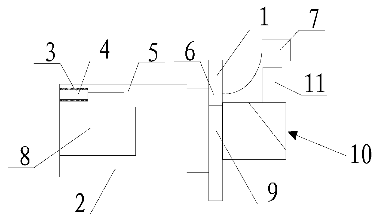
[0032] Such as Figure 5 The shown in-situ morphology and optical performance monitoring evaporation source are consistent with the basic structure of the evaporation source in Example 1, except that the optical component 10 is also connected to the spectrometer 12, and the spectrometer 12 is also connected to the detector 13, And it also includes a computer system 14, which is respectively connected with the imaging component and the detector for data collection and data processing. Simultaneous configuration of imaging component 11, spectrometer 12 and detector 13 can realize the associated evolution of morphology and optical properties, and can perform micro-area analysis on the surface of the film; after connecting with computer system 14, the measured data can be digitized, and Control, data acquisition, data processing, etc. for all operations through the same computer.

[0033] Install any in-situ morphology and optical performance monitoring evaporation source in Exam...


PUM


Abstract

The invention relates to an in-situ morphology and optical performance monitoring evaporation source. The in-situ morphology and optical performance monitoring evaporation source comprises a vacuum flange, a heat shielding assembly supported on any one side face of the vacuum flange, a heating assembly which is embedded at one end, which is far away from the vacuum flange, of the heat shielding assembly, a material container which is arranged in the heating assembly, a temperature measuring assembly which is mounted adjacently to the material container and is used for measuring the temperature, a vacuum electric connector which is respectively electrically connected with the heating assembly and the temperature measuring assembly and is mounted on the vacuum flange, and a control power source which is connected with the vacuum electric connector; the evaporation source further comprises a microscope mounted in the heat shielding assembly; and the vacuum flange is provided with an observation window which is opposite to the position of the microscope. The heat shielding assembly is internally provided with the microscope and the vacuum flange is provided with the observation window which is opposite to the position of the microscope, so that the morphology and the optical performance of a deposited material on the surface of a substrate can be monitored in real time when the evaporation material is deposited.

Description

technical field [0001] The invention relates to an evaporation source for in-situ morphology and optical performance monitoring, and also relates to a vacuum deposition device for in-situ morphology and optical performance monitoring. Background technique [0002] Thin film materials have a wide range of applications in various fields, such as anti-corrosion, anti-reflection, optical lenses, microelectronic devices and optoelectronics, etc. For now, people have developed a variety of methods to prepare thin film materials, such as vacuum thermal evaporation deposition, vacuum sputtering, spin coating, pulling, spraying and so on. For most optical and electronic devices, the requirements for the fabricated thin films are extremely high, such as uniformity, thickness control, impurity concentration, etc. Among the developed technologies, vacuum deposition technology is a conventional thin film fabrication method. Its advantages lie in the high quality of the film produced, ...

Claims


Application Information

Patent Timeline
Patent Type & Authority Applications(China)
IPC IPC(8): C23C14/52C23C14/24
Inventor 迟力峰王文冲
Owner SUZHOU UNIV
Why Eureka
Try Eureka