Critical size control system

A key size and control system technology, applied in semiconductor/solid-state device manufacturing, discharge tubes, electrical components, etc., can solve the problems of small critical size in the middle area of ​​the wafer, large critical size in the edge area, and high cost, and achieve the realization cost Small, easy to extend the effect of the application

Active Publication Date: 2014-05-21
ADVANCED MICRO FAB EQUIP INC CHINA
View PDF2 Cites 5 Cited by
  • Summary
  • Abstract
  • Description
  • Claims
  • Application Information

AI Technical Summary

Problems solved by technology

In the actual process, usually the temperature in the center of the reaction chamber is relatively high and the temperature in the edge is relatively low, which is likely to cause the critical dimension of the middle area of ​​the wafer to be small and the critical dimension of the edge area to be large, so that the critical dimensions of different areas of the wafer Dimensional loss of uniformity
[0004] Due to the precise requirements of the plasma treatment process and the process requirements that the critical dimensions of each area of ​​the wafer should be uniform, it is difficult to improve the reaction chamber itself in the existing technology to control the concentration distribution of the plasma in it, so as to achieve different wafers. Uniformity of area critical dimensions
Or, realizing this kind of regulation requires a large overhead, which increases the complexity of the process

Method used


Image

  • Critical size control system
  • Critical size control system
  • Critical size control system

Examples


Embodiment Construction

[0019] The specific embodiment of the present invention will be further described in detail below in conjunction with the accompanying drawings.

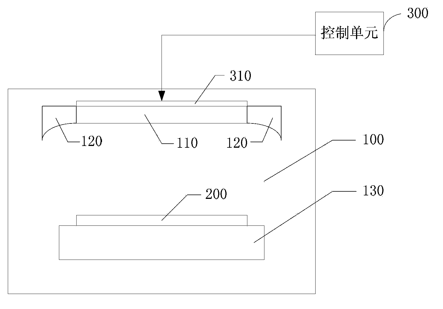
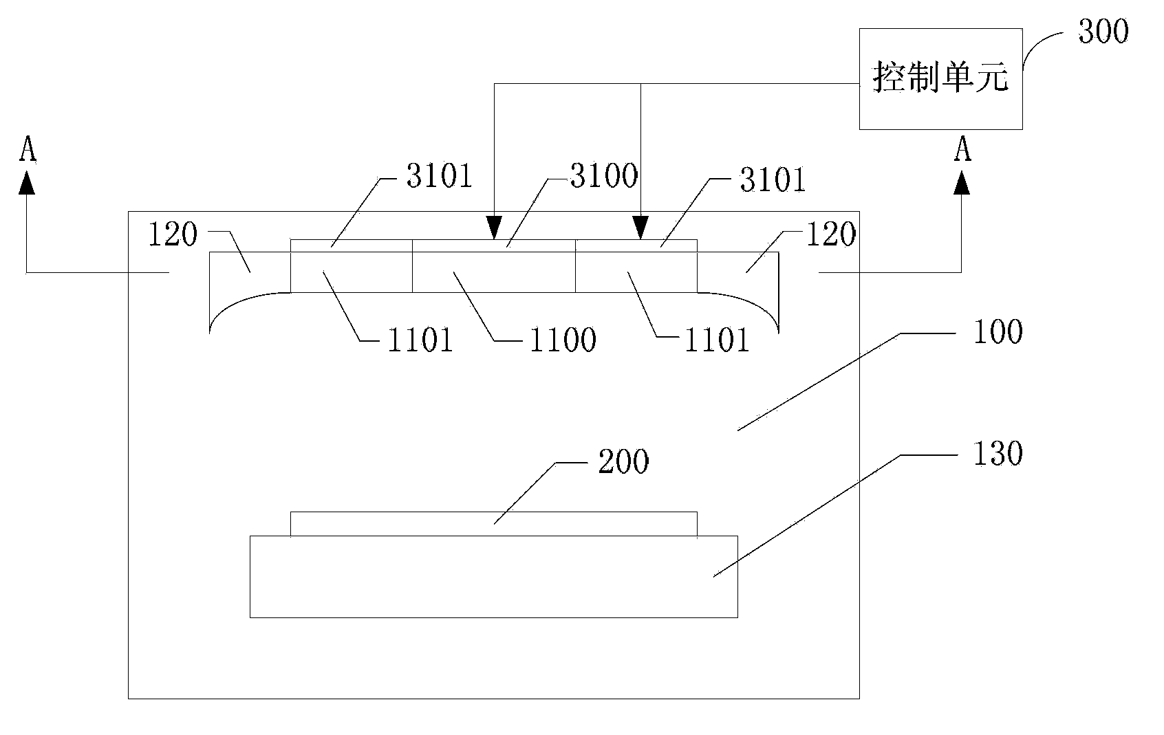
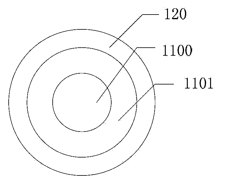
[0020] Such as figure 1 As shown, the first embodiment of the present invention is used to control the critical dimension of the wafer 200 in the plasma processing process. The plasma processing process is carried out in a reaction chamber 100, and the top of the reaction chamber 100 is provided with a gas shower head 110 and The ground ring 120 surrounds and supports the gas shower head 110 , and the carrying part 130 at the bottom of the reaction chamber 100 is used to carry the wafer 200 . The critical dimension control system provided by the first embodiment includes: a control unit 300 and a first temperature control device 310, wherein the first temperature control device 310 is composed of a first temperature control unit, and the first temperature control unit and the gas shower head 110 contacts.

[0021] Specifically, th...


PUM


Abstract

The invention relates to a critical size control system and a plasma processing device. The critical size control system comprises a first temperature control device and / or a second temperature control device and a control unit; the first temperature control device which is in contact with a gas spraying head is used for detecting, adjusting and controlling the temperature of the gas spraying head; the second temperature control device which is in contact with a grounding ring is used for detecting, adjusting and controlling the temperature of the grounding ring; the control unit which is corresponding to the first temperature device and / or the second temperature control device generates at least one type of the following control signals which comprise a first control signal which is used for controlling the first temperature control device to adjust the temperature of the gas spraying head and a second control signal which is used for controlling the second temperature device to adjust the temperature of the grounding ring. The critical size control system has the advantages of achieving adjusting and controlling of the critical size of different areas of wafers and being low in achieving costs and easy to expand and apply due to the temperature control of the gas spraying head and the grounding ring.

Description

technical field [0001] The present invention relates to the field of semiconductor manufacturing technology, and more specifically, to a critical dimension (Critical dimension, CD for short) control system. Background technique [0002] The plasma treatment process in the field of semiconductor processing is carried out in the reaction chamber. RF power is applied to the reaction chamber to form a radio frequency electric field in the reaction chamber, and the reaction gas mixed with various raw materials is introduced into the reaction chamber. , the reactive gas generates plasma under the action of a radio frequency electric field, and undergoes a plasma reaction with the wafer to be processed. [0003] In the processing process, in order to meet the process requirements, a large number of process parameters must be strictly controlled. The critical dimension of the wafer is one of the most important parameters. The temperature in the reaction chamber has the most signific...

Claims


Application Information

Patent Timeline
Patent Type & Authority Applications(China)
IPC IPC(8): H01L21/02H01J37/32
CPCH01J37/32954H01L21/67011H01L21/67248H01L21/67253
Inventor 杨平黄智林王兆祥杜若昕
Owner ADVANCED MICRO FAB EQUIP INC CHINA
Why Eureka
Try Eureka