IGBT power device for low power application and method of manufacturing the same
A technology of power device and manufacturing method, which is applied in the direction of semiconductor/solid-state device manufacturing, semiconductor device, electrical components, etc., to achieve the effect of improving turn-off time, turn-on and turn-off time
- Summary
- Abstract
- Description
- Claims
- Application Information
AI Technical Summary
Problems solved by technology
Method used
Image
Examples
Embodiment Construction
[0021] In order to facilitate those skilled in the art to further understand the present invention, clearly understand the technical solutions of the present invention, and fully and fully disclose the relevant technical content of the present invention, the specific embodiments of the present invention will be described in detail below with reference to the accompanying drawings. Of course The described specific embodiments only list a part of the embodiments of the present invention, rather than all the embodiments, to help understand the present invention and its core ideas.
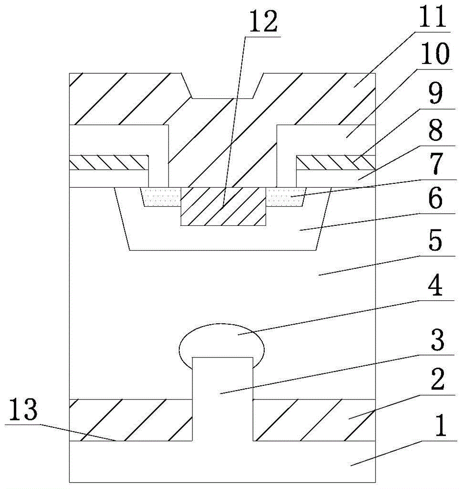
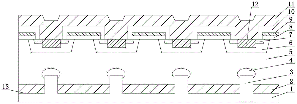
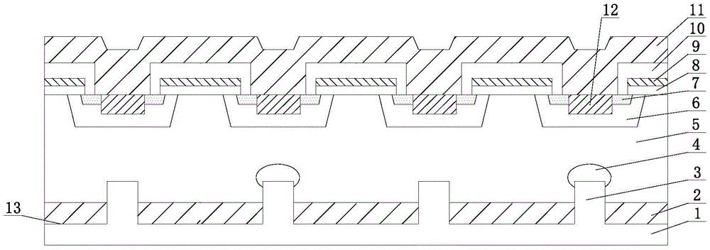
[0022] The basic idea of the present invention is to optimize the design of the backside structure of the IGBT, to increase the metal-filled trench without affecting the voltage resistance of the device itself, to heavily dope the P-type, and to only use the trench surface (especially the trench The bottom of the groove) is injected into the N-type region, the N-type region can also be arranged in a rep...
PUM
 Abstract
Description
Claims
Application Information


