Novel packaging method of MEMS (Micro-electromechanical Systems) structure and processing circuit integrated system

A technology for processing circuits and integrated systems, applied in the directions of microstructure devices, manufacturing microstructure devices, circuits, etc. Effect

Active Publication Date: 2014-05-28
BEIJING MXTRONICS CORP +1
View PDF5 Cites 14 Cited by
  • Summary
  • Abstract
  • Description
  • Claims
  • Application Information

AI Technical Summary

Problems solved by technology

In addition, according to the concept of wafer-level packaging, only wafer-level bonding technology has been realized in China at this stage, which cannot be equivalent to wafer-level packaging, because the symbol of wafer-level packaging is that once the chip is cut, it can be used normally without additional bonding wire
In China, there is a method of making holes on silicon and filling bumps to achieve wafer-level hermetic packaging. However, this method first thins the silicon cover to 120μm-160μm, and then opens the holes. The process is complicated and the yield is low.

Method used


Image

  • Novel packaging method of MEMS (Micro-electromechanical Systems) structure and processing circuit integrated system
  • Novel packaging method of MEMS (Micro-electromechanical Systems) structure and processing circuit integrated system
  • Novel packaging method of MEMS (Micro-electromechanical Systems) structure and processing circuit integrated system

Examples


Embodiment Construction

[0049] Below in conjunction with accompanying drawing and specific embodiment the present invention is described in further detail:

[0050] The novel packaging method of the MEMS structure and processing circuit integrated system of the present invention specifically comprises the following steps:

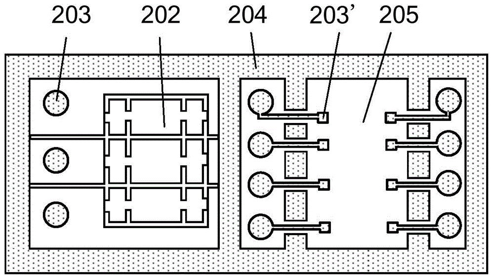
[0051] Step (1), forming a reserved circuit area 205 on the MEMS wafer

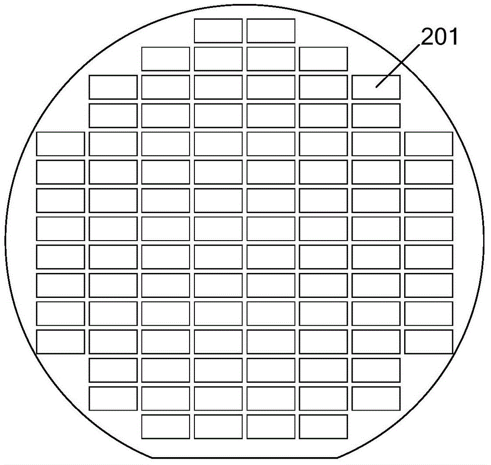
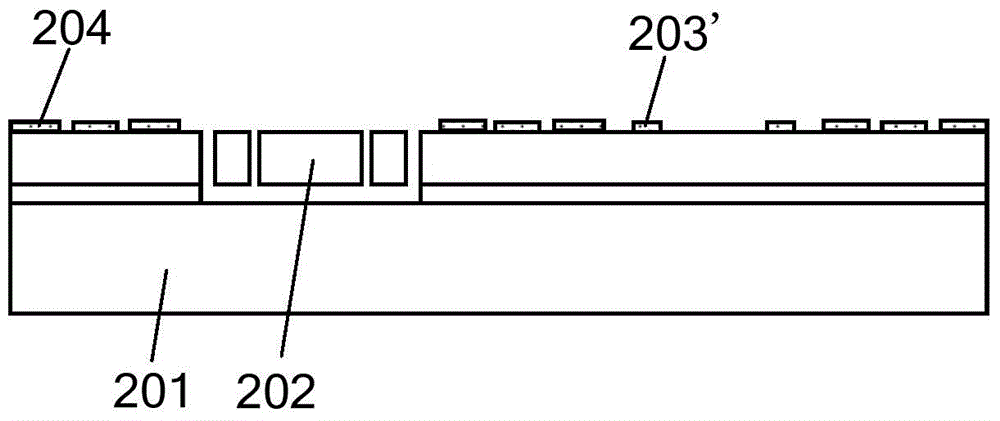
[0052] like figure 1 Shown is a schematic diagram of the distribution of the MEMS wafer before packaging in the present invention. It can be seen from the figure that the MEMS wafer includes N base units. like Figure 2A Shown is a top view of a single MEMS structure on the MEMS wafer before packaging of the present invention, Figure 2B It is a cross-sectional view of a single MEMS structure on a MEMS wafer before packaging in the present invention. On each base unit of the MEMS wafer substrate 201, the MEMS structure 202 is processed by the MEMS process, the metal film layer is formed on the substrate s...


PUM

PropertyMeasurementUnit
thicknessaaaaaaaaaa
thicknessaaaaaaaaaa
thicknessaaaaaaaaaa

Abstract

The invention relates to a novel packaging method of an MEMS (Micro-electromechanical Systems) structure and a processing circuit integrated system. The method comprises the following steps: (1) preserving a plurality of circuit chip holding areas on each substrate unit of an MEMS wafer, and putting circuit chips on the MEMS wafer to form integration of the MEMS structure with a processing circuit; (2) utilizing a vertical intercoupling technique, using silicon as a cover plate in which a vertical through hole is formed, filling a conductive material into the through hole to form an input port and an output port of the structure; (3) forming a plurality of grooves in the binding surface of the cover plate for providing a vacuum airtight environment necessary for working of an MEMS device and a space required by the circuit, wherein an air sucking agent film inside the cover plate groove is used for maintaining the vacuum degree; (4) performing wafer binding on the cover plate and the MEMS wafer so as to achieve the wafer grade vacuum integrated packaging. The method is not only simple in process, wide in application range and remarkable in effect, but also can avoid thermal stress caused by the coefficient of thermal expansion, and can remarkably improve the temperature coefficient of a device.

Description

technical field [0001] The invention relates to a system-integrated wafer-level vacuum packaging method, in particular to a novel packaging method for an MEMS structure and processing circuit integrated system. Background technique [0002] MEMS is the abbreviation of micro-mechanical electronic system, and the system integration of MEMS structure and processing circuit is the development goal of MEMS field. At present, there are MEMS devices that integrate MEMS structures and COMS circuits into one chip abroad, but this process is very complicated and is limited to some specific sensitive structures and circuits, such as silicon micro-microphones and other MEMS systems that use surface silicon technology. Not of general application. In addition, the integration of MEMS structures and processing circuits can also be achieved through device-level integrated packaging, that is, MEMS chips and processing circuits are packaged together in a package. This method has low integrat...

Claims


Application Information

Patent Timeline
Patent Type & Authority Applications(China)
IPC IPC(8): B81C1/00B81B7/00
Inventor 杨静张富强孟美玉李光北孙俊敏钟立志
Owner BEIJING MXTRONICS CORP
Why Eureka
Try Eureka