Method for reducing stress on peripheral region of silicon through hole

A surrounding area and through-silicon via technology, which is applied in the field of microelectronics, can solve the problems of adverse effects on the normal operation of adjacent devices with service life, great difficulty in technical realization, and complicated process, so as to overcome the complexity of the process and make the process simple and reliable , easy to achieve effect

Inactive Publication Date: 2014-05-28
NAT CENT FOR ADVANCED PACKAGING
View PDF4 Cites 12 Cited by
  • Summary
  • Abstract
  • Description
  • Claims
  • Application Information

AI Technical Summary

Problems solved by technology

However, the process of through-silicon vias is more complicated, mainly including silicon hole etching, insulating layer / barrier layer / seed layer deposition, through-hole filling, chemical mechanical polishing, wafer bonding, debonding, wafer thinning, metal Rewiring production, bump preparation, etc.
The above steps such as etching, via filling and subsequent heat treatment will cause a certain stress phenomenon in the surrounding area of ​​the TSV, especially the area within 50 microns, and this stress will affect the service life of the TSV and silicon. Adversely affect the normal operation of adjacent devices in the area outside the via
At present, the method of annealing copper is mainly used to reduce the stress around the hole and the range of stress influence (KOZ, Keep-Out-Zone). This method belongs to the traditional method. The heat treatment itself will bring a certain amount of stress, so it will affect the stress. the elimination of
The U.S. patent with the publication number US2013 / 0049220A1 proposes a solution to reduce the above-mentioned stress by setting stress plugs around the TSV and through a specific spatial arrangement of the two, but it is necessary to consider the direction of the silicon lattice. very difficult

Method used


Image

  • Method for reducing stress on peripheral region of silicon through hole
  • Method for reducing stress on peripheral region of silicon through hole
  • Method for reducing stress on peripheral region of silicon through hole

Examples


Embodiment Construction

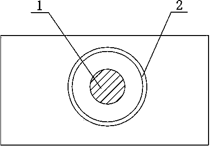
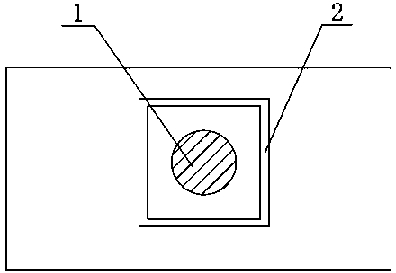
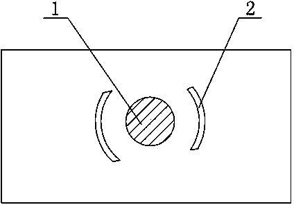
[0021] figure 1 Among them, 1 is a TSV, and 2 is a stress relief structure of an annular groove. The circular ring and the TSV are in a concentric circle structure, but in the actual design process, they may also be non-concentric circles. The distance between the annular groove 2 and the TSV 1 depends on factors such as the diameter and height of the TSV, usually in the range of 0-50 microns, and the depth of the annular groove 2 also depends on factors such as the diameter and height of the TSV , usually in the range of 0-100 microns. This stress relief structure is relatively uniform in stress relief in the area around the TSV, and is suitable for occasions where the device distribution is also relatively uniform. figure 2 and figure 1 Very similar, the difference is that a square groove 2 is used instead of an annular groove. image 3 Among them, 1 is a through-silicon via, and 2 is a stress relief structure of an unclosed arc-shaped groove. The arc-shaped grooves ar...


PUM


Abstract

The invention relates to a method for reducing stress on the peripheral region of a silicon through hole. The silicon through hole can be subjected to etching, side wall insulation, seed layer deposition, through hole filling and other process steps in a preparation process to generate process residual stress; in addition, the thermal expansion coefficient of copper is greatly different from that of a peripheral material, therefore, a certain stress concentration phenomenon is generated on the periphery region of the silicon through hole, and the stress can bring adverse effects on the performances and reliabilities of semiconductor devices around the silicon through hole. The invention provides a solution for processing a stress eliminating structure with a certain depth and specific shape within a certain region at the periphery of the silicon through hole in order to overcome the limitation of reducing the stress at the periphery of the hole and the stress influence range in an annealing way adopted at present. Compared with the prior art, the method has the beneficial effects that the process complexity of the annealing way for eliminating the stress is lowered, the area of a stress influence region is greatly reduced, the service life of the silicon through hole can be remarkably prolonged and the working stability of peripheral devices can be remarkably improved through arranging the specific stress eliminating structure within a certain region at the periphery of the silicon through hole by using the traditional etching way, and the method has the advantages of simple and reliable process and easiness for realization.

Description

technical field [0001] The invention relates to a method for manufacturing or processing semiconductor or solid devices in the technical field of microelectronics, in particular to a method for reducing the stress in the surrounding area of ​​a through-silicon hole. Background technique [0002] With the development of semiconductor technology, electronic devices are getting smaller and smaller, with higher integration, more and more functions included, and the overall performance of devices is getting stronger. The feature size of the semiconductor process has reached the nanometer level, and the limitations of the continuous proportional reduction of the integrated circuit are becoming more and more serious, and it is getting closer and closer to the physical limit. Therefore, high-density three-dimensional integration or 3D integration has become an important technical direction of microelectronic system-level integration, which can effectively meet the requirements of hi...

Claims


Application Information

Patent Timeline
Patent Type & Authority Applications(China)
IPC IPC(8): H01L21/02H01L21/768
CPCH01L21/76898H01L21/76829
Inventor 靖向萌于大全
Owner NAT CENT FOR ADVANCED PACKAGING
Why Eureka
Try Eureka